=================================================================================
Dynamical scattering exists in many cases. In the case of double diffraction, the wave is first diffracted by a set of parallel lattice planes (h1k1l1) and then by another set of planes (h2k2l2) according to the following equations,
h3 = h1 + h2 --------------------------------------- [2731a]
k3 = k1 + k2 --------------------------------------- [2731b]
l3 = l1 + l2 ----------------------------------------- [2731c]
where,
h k l -- Miller indices.
For instance, ±(002) reflections in the [110] orientation are examples of kinematically forbidden reflections in silicon (Si). However, in thick TEM specimen those reflections arise due to double scattering (double diffraction) by the ±(-111) and ±(1-11) reflections. They are also induced partially by the fact that the “geometrical part” of the Lorentz factor [1] may enhance their intensities since the four {111} reflections reflect the largest net-plane spacing in any <110> projection.
For hcp crystals, the (0 0 0 l) reflections, e.g. for the case with 164 (P-3m1) space group, are forbidden when l is odd. However, those reflection positions often show diffraction intensity, which is probably caused by chemical order on the basal planes, or by double or multiple diffraction (scattering).
Table 2731 lists more examples of double/multiple diffractions with "thick" TEM specimens.
Table 2731. Examples of double/multiple diffractions with "thick" TEM specimens.
| * E.g. (01-11) + (0-110) → (0001) |
Note that for electron diffraction, if the specimen has thickness gradient, the thicker part shows intensities in the forbidden reflections, indicating multiple diffractions while the thinner part shows zero intensity in the same type of reflections.
Figure 2731a shows an SAED pattern of hexagonal La3Cu2VO9 (a ≈ 14.4 Å and c ≈ 10.7 Å) crystals in space group P63/m. The SAED pattern presents the only forbidden spots along c axis (000l spots with odd l) which were found by tilting the TEM specimen. The same forbidden spots were found in [1-100] zone axis as well; however, there were no visible double diffraction spots. Therefore, the visibility of double diffraction spots depends on specimen thickness as well as zone-axis.
Figure 2731a. [11-20] SAED pattern of hexagonal La3Cu2VO9. The small arrows denote the forbidden reflections visible due to double diffraction. Adapted from [1]
Figure 2731b shows a selected area electron diffraction (SAED) pattern of an Bi12.8Co0.2Mo5O34±δ (a = 11.7226(6) Å; b = 5.7959(2) Å; c = 24.6994(11)Å; β = 102.08(1)°, space group P2/c (13)) crystal taken along [010] and [100] zone axes. The forbidden reflections still appeared due to double diffraction. However, this effect disappeared when the crystal was tilted away from the perfect zone axis orientation because the specimen was not very thick (see discussion below).
Figure 2731b. Selected area electron diffraction (SAED) pattern of an Bi12.8Co0.2Mo5O34±δ crystal taken along [010] (a) and [100] (b) zone axes. Adapted from [2]
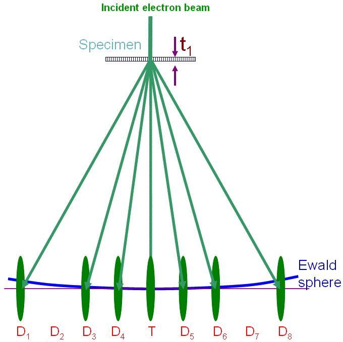
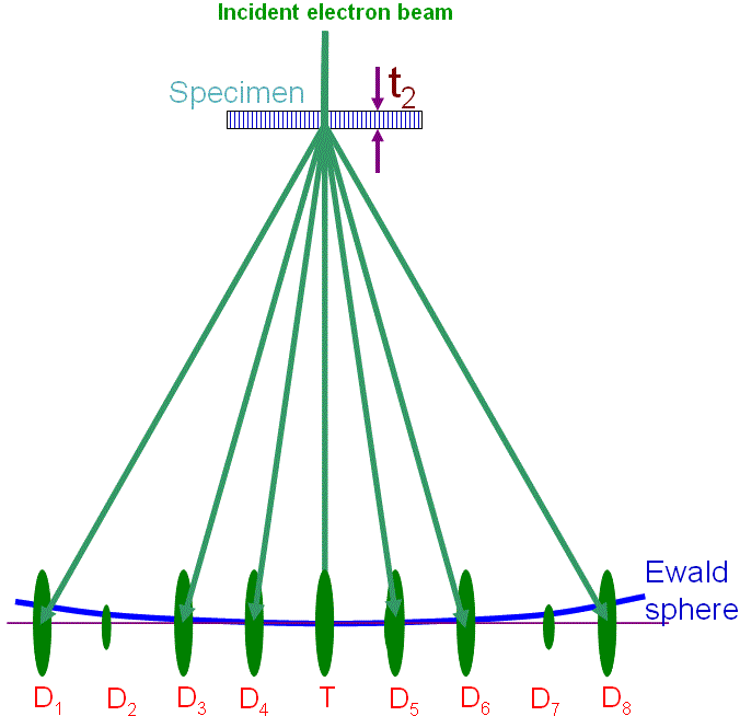
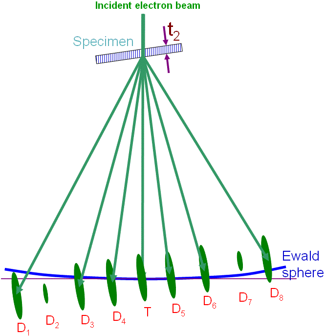
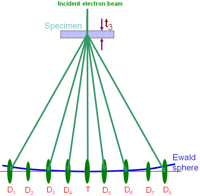
Figure 2731c shows the schematic illustration of the reflection- and forbidden-relrods of zone axis diffraction patterns at different specimen thickness. At zero tilt, the Ewald sphere is tangential to zero-order Laue zone (ZOLZ) of the reciprocal lattices in Figures 2731c (a), (b) and (d). For very thin specimens, the forbidden-relrods (D2 and D7) do not appear as shown in Figure 2731c (a), while they appear when the thickness of the specimens increases as shown in Figure 2731c (b) and (d) and the visible forbidden-relrods elongate more for thicker specimens. Note that the forbidden-relrods become visible due to double diffraction in thicker specimens. When the specimen is tilted, the loci of the intersections of Ewald sphere with the relrods does not change, and thus the projected positions of reflections do not move. However, the excitation errors (s) for the relrods change significantly, so that reflection intensities in the electron diffraction patterns change significantly. Especially, for the relatively thin specimen as shown in Figure 2731c (c), the forbidden-relrods (D2 and D7) will disappear on the recorded diffraction pattern (intersections of Ewald sphere with the relrods) because they are too short to appear with specimen-tilting. However, for very thick specimens as shown in 2731c (d), both the reflection- and forbidden-relrods are almost in the same length so that the forbidden-relrods will not disappear before reflection-relrods with specimen-tilting.
Figure 2731c. Schematic illustration of reflection- and forbidden-relrods of zero-order Laue zone (ZOLZ), depending on film thickness and specimen tilting: (a) At zero tilt, very thin TEM specimen for which forbidden-relrods do not exist; (b) At zero tilt and (c) at high-angle tilt, not very thin TEM specimen for which short forbidden-relrods appear; and (c) At zero tilt, very thick TEM specimen for which long forbidden-relrods appear. Here, t1 < t2 < t3.
[1] Moeck, P.; Rouvimov, S.: Structural fingerprinting of nanocrystals
in the transmission electron microscope: utilizing information
on projected reciprocal lattice geometry, 2D symmetry, and
structure factors. In: Drug Delivery Nanoparticles Formulation
and Characterization (Eds. Y. Pathak, D. Thassu), Informa,
2009 (Drugs and the Pharmaceutical Sciences, Vol. 191), pp.
270–313, (ISBN-13: 978-1-4200-7804-6).
[2] Z. A. Mikhailovskaya, E. S. Buyanova, S. A. Petrova, M. V. Morozova, V. M. Zhukovskiy, R.G. Zakharov, N. V. Tarakina, I. F. Berger, Cobalt-doped Bi26Mo10O69: Crystal structure and conductivity, Journal of Solid State Chemistry 204 (2013) 9–15.
|
![[11-20] SAED pattern of La3Cu2VO9](image2/1878a.GIF)
![Selected area electron diffraction (SAED) pattern of an Bi12.8Co0.2Mo5O34±δ crystal taken along [100] zone axis](image2/1668b.GIF)
![Selected area electron diffraction (SAED) pattern of an Bi12.8Co0.2Mo5O34±δ crystal taken along [100] zone axis](image2/1668.GIF)