Chapter/Index: Introduction | A | B | C | D | E | F | G | H | I | J | K | L | M | N | O | P | Q | R | S | T | U | V | W | X | Y | Z | Appendix
|
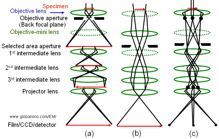
Diffraction requires "coherent scattering", which is characterized by a precise relationship between the phases of the incident and scattered waves. Simply speaking, the elastic scattering of electrons occurs mainly from electron interaction with the atomic nuclei or the whole electrostatic field of the atoms. The elastic scattering is responsible for electron diffraction from the specimen in TEM. The physical process of the electron diffraction is described mathematically by a Fourier transform. Electrons are scattered at the energy distribution of electrostatic potential within the unit cell. This distribution peaks at the positions of atoms. For TEM, because the crystal is a three-dimensional (3-D) structure, the reciprocal lattice is also a 3-D array of reflection points. The reflection signal (diffraction spots) shows up when the Ewald sphere intersects the reciprocal-lattice points (the Bragg condition is satisfied). You should always imagine that the position of the reflected spot is in 3-D lattice, especially when you are studying crystallography of nanomaterials and small defects in crystals. In the case of TEM thin film, reflected relrods are formed. When the specimen or the electron beam is tilted, the spot position in the diffraction pattern moves because the Ewald sphere moves relative to the reciprocal lattice. Note that due to the small wavelength of electrons in TEM, the radius of the Ewald’s sphere is much larger than that of X-ray so that more reflected spots appear on the TEM screen or detector. Figure 4107a presents the difference of lens settings between TEM image modes and diffraction mode. Figure 4107a (a) shows the principle of magnifying an image (Normal-Mag mode). A transmitted image of the specimen is first formed and magnified by the objective lens, and then is magnified further by two to four lenses, including an objective lens, intermediate lenses, and a projector lens. As shown in Figure 4107a (b), at extremely low magnification (e.g. used for survey of interest), the image is formed by the OM (objective-mini) lens, intermediate lenses, and projector lens. The Diff mode in Figure 4107a (c)presents an electron diffraction pattern. In the Normal-Mag mode, the focus of the 1st intermediate lens is adjusted to the image plane of the objective lens where a selected area aperture is located. However, in the Diff mode, the focus of the 1st intermediate lens is adjusted at the back focal plane of the objective lens. Table 4107 lists the status of the lenses and apertures in different operation modes.
Figure 4107a. (a) Normal-Mag mode, (b) Low-Mag mode, and (c) Diff mode. The dashed-lenses are turned off in the relevant operation mode. Table 4107. Status of the lenses and apertures in different operation modes*.
If there is no intermediate lens, then by switching to diffraction mode, the focus of the projection lenses can be changed in order to focus on the back focal plane of the objective lens. The selected area diffraction (SAD) aperture is used to exclude parts of the area being viewed so that we can make sure the diffraction pattern originates from a small, specific area. In principle, the diffraction spots become infinitely small when the specimen is illuminated by a parallel electron beam. Figure 4107b shows angular distributions of elastically scattered electrons, forming electron diffraction patterns, as a function of scattering angle in TEMs. 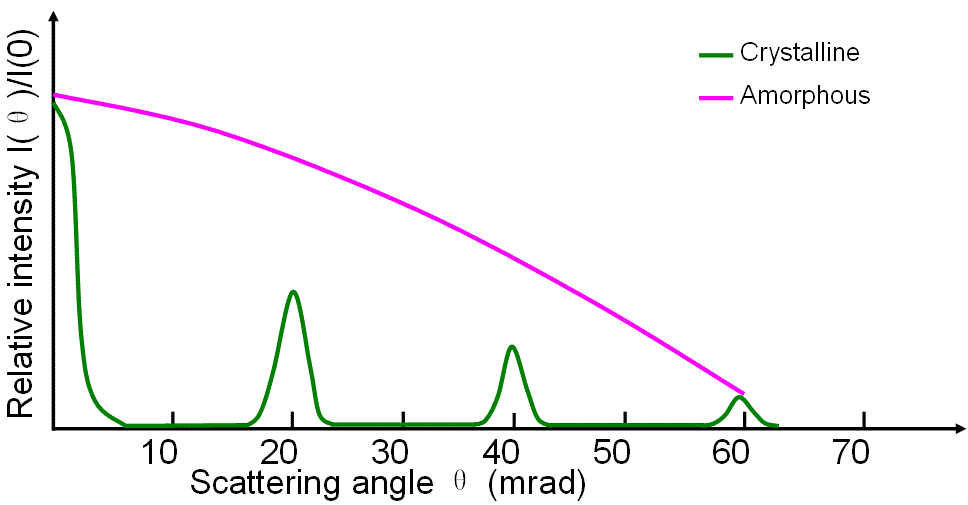 Figure 4107b. Elastic scattering of electrons with crystalline and amorphous specimens. In electron diffraction techniques (e.g. SAED and NBD), a camera length of ~500 mm is commonly used, but it can be changed depending on whether or not we want to observe the details in HOLZ. It’s quite practical that we always use a specific value of L on a particular TEM system. We may increase the L for special analysis of high-resolution diffraction, but will exclude a large number of other reflections. Note that the RDF analysis is important for the study of non-crystalline solids. The RDFs can be experimentally measured after Fourier transformation of neutron or electron diffraction or X-ray diffraction (XRD) data.
|