=================================================================================
The lattice constant of fully relaxed Si1-xGex crystal (aSiGe) is given by the modified Vegard's law,
aSiGe = aGeX + aSi(1-X) - 0.0272 X(1-X)
= 0.5431 + 0.01992 X + 0.002733 X2 (nm) ---------------------- [3380a]
where,
aGe -- The lattice constant of pure Ge crystal.
aSi -- The lattice constant of pure Si crystal.
As discussed in page3381, for the (001) SiGe/Si system in which the primary misfit dislocations are <110>{111}, the critical thickness hc of SiGe epitaxial layer without misfit dislocations can be given by, [1]
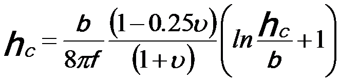 ---------------- [3380b] ---------------- [3380b]
However, the actual lattice-mismatched SiGe films can be grown thicker than predicted without misfit dislocations. The empirical critical thickness is approximately 1.65 times that predicted by Equation 3380b.
Other factors can also determine the defect density in the strained epitaxial films. For instance, the defect density decreases as the single crystal area decreases.
Figures 3380a and 3380b show the features of dislocations in SiGe epitaxial films on Si substrates depending on the sizes of the active areas of microelectronic devices. The black surroundings are Si substrate.
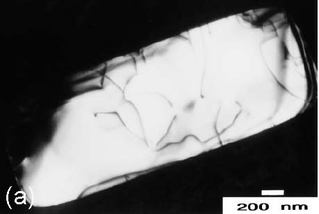 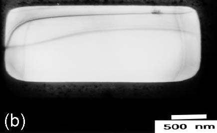
Figure 3380a. Dislocations in smal active areas: (a) Stressed-isolation wafer with 0% Ge,
(b) Relaxed-isolation wafer with 13% Ge, after the 950 °C anneal. Adapted from [2]
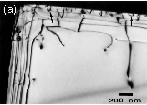 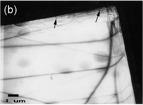
Figure 3380b. Dislocations in large active areas (37 µm x 180 µm): (a) Stressed-isolation wafer; (b) Stressed isolation wafer with 0% Ge after the 950 °C anneal. Note that the arrows indicate the dislocation loops at the edge of the active areas. The density of dislocations at the isolation edge is high and there is no dislocations in the center region. Adapted from [2]
Table 3380. Comparison of properties of crystalline and amorphous SiGe materials.
|
Crystalline SiGe |
Amorphous SiGe |
Energy gap/Optical band gap Eg (eV) |
|
1.50 for a-Si1-xGex:H |
Urbach energy E0 (meV) |
|
50 for a-Si1-xGex:H |
Fermi level density of states g (EF) (cm-3eV-1) |
|
1016 for a-Si1-xGex:H |
[1] S. R. Stiffler, J. Comfort, C. L. Stanis, D. L. Harame, E. de Frésart, and B. S. Meyerson, J. Appl. Phys. 70, 1416 (1991).
[2] K. Schonenberg, Siu-Wai Chan, D. Harame, M. Gilbert, C. Stanis and L. Gignac, The stability of Si1−xGex strained layers on small-area trench-isolated silicon, Journal of Materials Research, 12(02) (1997), pp 364-370.
|