=================================================================================
Page2393 lists the properties of single-crystalline, polycrystalline, and amorphous silicon (Si) materials.
Table 2019a. Bond density (x1015/cm2) of various Si crystal planes.
Plane |
In-plane |
Surface |
Total |
(110) |
0.96 |
0.96 |
1.92 |
(522) |
0.35 |
1.06 |
1.41 |
(100) |
0.00 |
1.36 |
1.36 |
(111) |
0.00 |
0.78 |
0.78 |
* The direction of the closest Si atoms in the {111} planes is along <110>.
Table 2019b. Relationship between resistivity (Ωcm) and dopant concentration (cm-3
) for crystalline Si at 23 °C.
Doping concentration |
Phosphorus, n-type |
Boron, p-type |
1012
|
3.8 x 10³ |
1.3 x 10⁴ |
1013 |
4.0 x 10² |
1.3 x 10³ |
1014 |
4.3 x 101 |
1.30 x 10² |
1015 |
4.5 |
1.4 x 101 |
1016 |
0.52
|
1.5 |
1017 |
8.5 x 10⁻²
|
0.2 |
1018 |
2.3 x 10⁻² |
4.5 x 10⁻² |
1019 |
5.5 x 10⁻³ |
8.5 x 10⁻³ |
1020 |
7.8 x 10⁻⁴ |
1.2 x 10⁻³ |
1021 |
1.2 x 10⁻⁴ |
1.3 x 10⁻⁴ |
Table 2019c. Surface energies (J/m2) of low-index Si surfaces. The types of reconstructions are indicated. (1x1) relaxed denotes an unreconstructed cleavage surface.
Solid |
(100)
|
(110)
|
(111) |
(522) |
Si |
1.41 c(4 × 4) |
1.7 (1 × 1) relaxed |
1.36 7 × 7 |
|
Si |
2.13 at 77 K
|
1.51 at 77 K |
1.23 at 77 K |
1.56 |
Table 2019d. Other properties of crystalline Si surfaces.
|
(100)
|
(110) |
(111) |
Atomic density (1014/cm2) |
6.78 |
9.59 |
15.66 |
Interatomic spacing (Å) |
|
1.36 |
|
Lattice spacing/constant (Å) |
5.43 |
3.84 |
3.13 |
Feature |
|
Si dumbbells |
|
Figure 2019a shows the absorption coefficient of silicon (Si) at 300 K. Note that the band gap of Si is about 1100 nm.
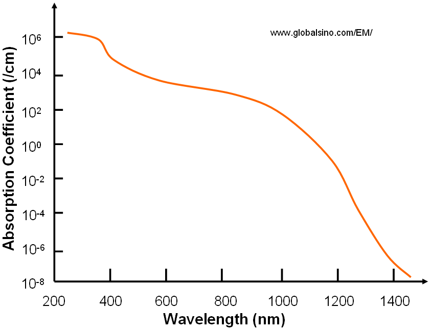
Figure 2019a. Absorption coefficient of silicon at 300 K.
Crystalline Si has the space group of Fd-3m (see in Table 2019a) and the space group for GaAs and InP is F-43m. Both these space groups are simple face-centred cubic (fcc) lattices.
Table 2019e. Etchants used in semiconductor manufacturing.
Film |
Etchant |
SiO2(Silicon oxide) |
Dilute hydrofluoric acid (DHF) |
Buffered HF (BHF) |
Polysilicon |
Alkaline hydroxide + organic |
Si3N4(silicon nitride)-selective to SiO2 |
Boiling phosphoric acid (H3PO4) |
Si3N4/SiO2 (non-selective) |
Hydrofluoric acid + organic |
Table 2019f. Etching selectivity of Si3N4:SiO2:Si in various solutions.
|
Etching selectivity of Si3N4:SiO2:Si |
BHF |
1:200:0 |
| 40% HF |
1:≥110:0.1 |
H3PO4 |
10:1:0.3 |
CF4-4% O2 plasma |
3:2.5:17 |
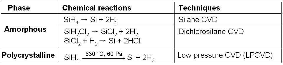
Table 2019g lists silicon wafers used in different technologies, and Table 2019h lists the chemical reactions used in CVD for Si film growth.
Table 2019g. Silicon wafers used in different device technologies.
Period
|
Wafer diameter |
Wafer thickness (μm) |
| (inch) |
(mm) |
|
| |
1 |
25 |
|
| |
2 |
51 |
275 |
1970-1975
|
3 |
76 |
375 |
| 1975-1980 |
4 |
100 |
450-500 |
| 1980-1985 |
4.9?or 5 |
125 or 130 |
525-625 |
| 1985-1990 |
~6 (5.9) |
150 |
675 |
| 1990-1995 |
~8 (7.9) |
200 |
725 |
| 1995-present |
~12 (11.8) |
300 |
770 |
|
~18 (17.7) |
450 |
925 |
Table 2019h. Chemical reactions used in CVD for Si film growth.
As listed in Table 2019i, substances with large bonding energies usually have high melting temperatures.
Table 2019i. Bonding energies and melting temperatures of covalent substances.
Bonding type |
Substance |
Bonding energy |
Melting point (°C) |
| kJ/mol |
kcal/mol |
eV/Atom, Ion, or Molecule |
Covalent
|
Typical value |
200-1000 |
|
|
|
| Si |
450 |
108 |
4.7 |
1410 |
| Diamond C |
713 |
170 |
7.4 |
>3550 |
Table 2019j. Comparison of properties between single, polycrystalline, and amorphous Si.
|
Single-crystal |
Poly-crystal |
Amorphous Si |
Basics |
|
|
|
|
|
|
|
|
Atomic properties |
Atomic number |
14 |
Electron Shells |
1s22s22p63s23p2 |
|
Radius of Si atom |
1.18 Å |
|
Structure |
Cubic, diamond |
|
Densest planes of Si atoms |
{111} planes |
|
Common Ions |
Si4+, Si4- |
|
Atomic density
(atoms/cm3) |
4.96 x 10²² |
|
Bond angle of adjacent atoms |
109 ° |
|
|
Deviation of bond angles |
|
±10° of ideal crystalline Si bond angle |
Deviation of bond lengths |
|
±2% of ideal crystalline Si bond length |
Density at 300K (g/cm3) |
2.329 |
|
Atomic weight |
28.09 g/g-mol |
Lattice spacing (a0 ) at 300K |
0.54311 nm |
|
Number of atoms in 1 cm3 |
4.995 x 10²² |
|
Distance between two neighboring atoms |
2.35 Å |
|
Atoms per unit cell |
8 |
|
Space Group |
|
|
Effective masses of heavy holes (mhh/m0) |
0.49 |
|
|
Effective masses of light holes (mlh/m0) |
0.16 |
|
|
Defect density |
|
|
10-15 cm-1 for a-Si:H-10 at.% |
Effective masses of (100) electrons in longitudinal direction (ml/m0) |
0.98 |
|
|
Effective masses of (100) electrons in transverse direction (mt/m0) |
0.19 |
|
|
Radiative recombination coefficient (cm3s−1) |
1.1 × 10⁻¹⁴ |
|
|
Mechanical properties |
Piezoresistive coefficient |
n-Si: p11 = -102
p-Si: p44 = +138
Gauge factor of 90 |
Gauge factor of 30 - 50 |
|
Fracture strength (GPa) |
6 |
0.8 to 2.84 (undoped) |
|
Residual stress
|
None |
Depending on structure; compressive |
|
Poisson ratio
|
0.262 maximum for (111) |
0.23 |
|
Young's modulus (N/m2) |
1.90 x 10¹¹ for (111) |
1.61 x 10¹¹ |
|
Elastic constant (dyn cm-2) |
C11=16.6 ×10⁻¹¹ at 300 K; C12=6.4 ×10⁻¹¹ at 300 K; C44=7.96 ×10⁻¹¹ at 300 K |
|
|
Thermal properties |
Thermal conductivity (W/cm-°C) |
1.5-1.57 |
Smaller for poly-Si films with fine grains and much greater with large grains |
|
Thermal expansion (/°C) |
2.3 |
2-2.7 |
|
Specific heat (cal/g-°C) |
0.169 |
|
Boiling point |
2480 °C |
|
|
Melting temperature |
1412 °C |
|
|
Melt heat (Qm, J-g-1) |
337 |
Critical temperature |
4920 °C |
|
|
Vapor pressure (Pa) |
1 at 1,650 °C; 10-6 at 900 °C |
|
|
Vaporization temperature (Tv, °C) |
2355 |
Vaporization heat (Qv, J-g-1) |
1446 |
Critical pressure (atm) |
1450 |
|
|
Coefficient of thermal expansion (CTE) (°C-1) |
(2.6 - 4.68)
x 10-6 for average between 15-1000 °C; 4.2 x 10⁻⁶ at 25 °C; zero at -157 °C; negative at liquid air temperature |
|
|
Thermal diffusion coefficient (cm2/s)
|
0.9 |
|
|
Entropy at 298 °K |
4.5 cal/mol/°K |
|
|
Diffusion length |
|
|
300 nm for a-Si:H-10 at.% |
Hole diffusion length |
|
|
1 µm for a-Si:H-10 at.% |
Optical properties |
Refractive index |
3.42 - 3.44 |
4.05 at 500 nm;
4.1 at 600 nm; 3.93 after deposition at T < 580 °C; 3.51 after deposition at T > 600 °C |
|
Cathodoluminescence (minimum voltage for excitation) |
2400 |
|
1600 |
Photoluminescence peak |
|
|
1.25 eV for a-Si:H(F)-10 at.% at 77 K |
Color |
Dark, steel gray for single crystal; Black, six-sided plates for graphitoidal Si; |
Transparent or light orange for small crystal (similar to c-Si film); |
Dark brown |
Absorption coefficient
(cm-1)
|
|
5.82 x 10⁶ at 3.5 eV |
|
Pre-exponent conductivity factor (Ω-1-cm-1) |
|
|
>103 for a-Si:H(F)-10 at.% |
Energy gap/Optical band gap Eg (eV) |
1.12 at 300 K; 1.17 at 0 K (Minimum indirect Eg) |
1.6 at 210 °C; 2.0 at 350 °C; |
1.55 for a-Si;
1.68 for a-Si:H,F;
1.7 - 1.8 for a-Si:H-10 at.% at 300 K |
Indirect bandgap (Eg,ind, eV) |
1.12 |
|
|
Direct bandgap (Eg, dir, eV) |
3.2 |
|
|
Variation of optical band gap with temperature
(eV-K-1) |
|
|
2x - 4x 10⁻⁴ |
ESR spin density (cm-3) |
|
|
1015 for a-Si:H(F)-10 at.% |
Spin–orbit splitting (eV) |
0.044 |
|
|
Infra-red spectra |
|
|
2000/640 cm-1 for a-Si:H(F)-10 at.% |
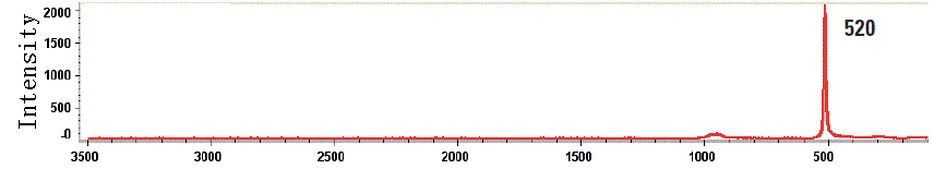
Raman spectra |
 |
|
|
Optical phonon energy (meV) |
64 |
|
|
Electrical properties |
Conduction band tail slope (meV) |
|
|
25 for a-Si:H(F)-10 at.%; 30 for a-Si |
Valence band tail slope (meV) |
|
|
40 for a-Si:H(F)-10 at.%; 50 for a-Si |
Activation energy (ΔE) |
|
≤0.05
for n-type a-Si:H ~1% addition of PH3 to gas phase; ≤0.05 for p-type a-Si:H ~1% addition of B2H6 to gas phase |
0.8 - 0.9 for a-Si:H(F)-10 at.%; 0.2 for n-type a-Si:H ~1% addition of PH3 to gas phase; 0.3 for p-type a-Si:H ~1% addition of B2H6 to gas phase |
Urbach energy E0 (meV)
|
|
|
46 for a-Si:H; 48 for a-Si:H,F |
Electron affinity |
4.05 eV |
|
|
Density of states
in band gap (cm-3) |
|
|
1 x 10¹⁹ for a-Si; 1 x 10¹⁶ for a-Si:H |
Energy gap at Γ (eV) |
3.5 |
|
|
Density of states at the minimum (cm-3eV-1) |
|
|
>1015 – 1017 for a-Si:H(F)-10 at.% |
Fermi level density of states g (EF) (cm-3eV-1)
|
|
|
1015 for a-Si:H; 1015 for a-Si:H,F |
Effective density of states at the conduction band edge
(Nc, cm-3eV-1) |
2.8 x 10¹⁹ at 300 K |
|
1021 for a-Si:H(F)-10 at.% |
Effective density of states at the valence band edge
(Nv, cm-3eV-1) |
1.04 x 10¹⁹at 300 K |
|
|
Extended state mobility: electron (cm2s-1V-1) |
|
|
>10 for a-Si:H(F)-10 at.% |
Extended state mobility: hole (cm2s-1V-1) |
|
|
~1 for a-Si:H(F)-10 at.% |
Hole drift
mobility µh
(cm2V-1s-1) |
450-600 |
|
10-20
for a-Si:H; 10-2 for a-Si:H(F)-10 at.% |
Electron drift
mobility µe
(cm2V-1s-1) |
≤1500 |
20 - 40 |
1 for a-Si:H-10 at.% |
Intrinsic carrier concentration ni |
1.0 x 1010 cm-3 |
|
|
Minority carrier lifetime |
2.5 x 10⁻³ s |
8 x 10-11 for grain size 0.2 µm; 7 x 10⁻⁶ for grain size 4,000 µm |
|
Intrinsic Debye length |
24 µm |
|
|
Dielectric Constant at 300 K |
11.9 |
|
|
Temperature resistivity coefficient (TCR, °C-1)
|
p-type: 0.0017 |
Nonlinear; e.g. 0.0012; between negative and positive depending on doping level |
|
Dark conductivity
(Ω-1-cm-1)
|
|
≥1 for n-type a-Si:H: ~1% addition of PH3 to gas phase; ≥1 for p-type a-Si:H: ~1% addition of B2H6 to gas phase |
10-10 for a-Si:H(F)-10 at.% at 300 K; 10-2 for n-type a-Si:H: ~1% addition of PH3 to gas phase; 10-3 for p-type a-Si:H: ~1% addition of B2H6 to gas phase |
Electrical resistivity (Ω-cm) |
Depending on doping level at room temperature; 2 x 10³ at -190°C; (2.3 - 3.2) x 105 at 22 °C; 15 at 300 °C; 0.4 at 500 °C |
Strong function of the grain structure of the film; always higher than that of Si single crystals; 4 x 10⁵ for doping level <1015 cm-3;
|
1011 for undoped a-Si:H-10 at.% at 300 K; 102 for n+ a-Si:H-10 at.% at 300 K;
103 for p+ a-Si:H-10 at.% at 300 K |
Breakdown field |
3 x 10⁵ V/cm |
|
|
Electron diffusion constant |
34.6 cm2s-1 |
|
|
Hole diffusion constant |
12.3 cm2s-1 |
|
|
|
Table 2019k lists the angles (2θB) between the direct beam 000 and diffracted beams as well as the lattice spacings for Si at accelerating voltages of 200, 300 and 400 kV. The angles can be computed with the DM scripts in the table.
Table 2019k. Reflection angles for silicon (Si,
a = 5.431195(9) Å).
hkl |
Reflection angles (1° = 17.45 mrad) |
Lattice spacing (nm) |
Forbidden reflections |
|
|
| 200 kV |
300 kV |
400 kV |
λ = 1.5405929 Å and T = 295.6 K |
111 |
8.01 mrad |
6.28 mrad |
5.23 mrad |
28.441° |
0.3135 |
|
200 |
|
|
|
|
|
Presents in [110] orientation due to double diffraction |
220 |
13.07 mrad |
10.26 mrad |
8.54 mrad |
47.300° |
0.1920 |
|
311 |
15.33 mrad |
12.03 mrad |
10.02 mrad |
56.120° |
0.1637 |
|
222 |
16.00 mrad |
|
|
|
0.1568 |
Forbidden |
400 |
18.49 mrad |
14.51 mrad |
12.08 mrad |
69.126° |
0.1358 |
|
331 |
20.67 mrad |
15.81 mrad |
13.16 mrad |
76.372° |
0.1246 |
|
422 |
22.65 mrad |
17.77 mrad |
14.80 mrad |
88.025° |
0.1108 |
|
511/333 |
24.02 mrad |
18.85 mrad |
15.69 mrad |
94.947° |
0.1045 |
|
440 |
|
|
|
106.701° |
|
|
531 |
|
|
|
114.084° |
|
|
620 |
|
|
|
127.534° |
|
|
533 |
|
|
|
136.880° |
|
|
622 |
30.66 mrad |
24.07 mrad |
20.03 mrad |
|
0.0819 |
Forbidden |
444 |
|
|
|
158.603° |
|
|
hkl |
|
|
|
|
|
h, k, l are mixed odd and even; or, all even and h + k + l ≠ 4n (Or defined by h + k + l = 4n + 2) |
The valence band electrons normally originate from the electrons in the incomplete outer shell of atoms, for instance, the valence band is formed for silicon (Si) crystals as shown in Figure 2019b. An isolated Si atom contains 14 electrons, which occupy 1s, 2s, 2p, 3s and 3p orbital in pairs. When atoms are far away from each other, the electrons in the out shell do not interact. As the distance between atoms is reduced to d1, there is an overlap of electron wavefunctions across adjacent atoms. This leads to a splitting of the energy levels consistent with Pauli exclusion principle, and forming energy bands. This splitting leads to 2N states in the 3s band and 6N states in the 3p band, where N is the number of Si atoms in the crystal. A further reduction of the lattice spacing causes the 3s and 3p energy bands to merge into a single band having 8N available states, and then split again into two bands containing 4N states each. At the temperature of zero Kelvin, the lower band is completely filled with electrons and named as the valence band. The upper band is empty and named as the conduction band. Note that in crystal Si (with lattice spacing d0), the core level electrons do not start yet to interact.
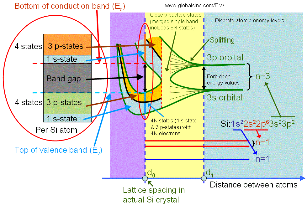
Figure 2019b. Detailed illustration of electronic structure of silicon as a function of distance between atoms. The left red circle is a zoom-in of the right red circle.
|
