=================================================================================
ELNES mapping is enabled by the fact that chemical bonding and short-range order in the environment of a specific chemical element induce a chemical shift of the energy-loss edge in the range between 0.1 and 8 eV and modifies the near-edge fine structure (ELNES) of the electron energy-loss spectrum. Therefore this method can differentiate between compounds of the same binary or multi-component system but with different bonding and valency.
Figure 3391a shows the Si L2,3 EEL spectra of Si, SiO2 and Si3N4. The positions of the edge onsets clearly indicate chemical shifts and differences in ELNES present. In Figure 3391a, for pure Si, the ELNES shows a first peak at 101.5 eV followed by a small plateau between 105 and 114 eV, and a very broad peak with the maximum at 135 eV. The SiO2 ELNES has a strong peak at 108.5 eV, which is also followed by a small plateau between 112 and 116 eV. However, the second peak located at 128 eV is far less intensive than the one for Si. An additional small peak presents at 161 eV. The ELNES of Si3N4 is very similar to the SiO2 ELNES. The two main peaks are located at 105 and 124.5 eV.
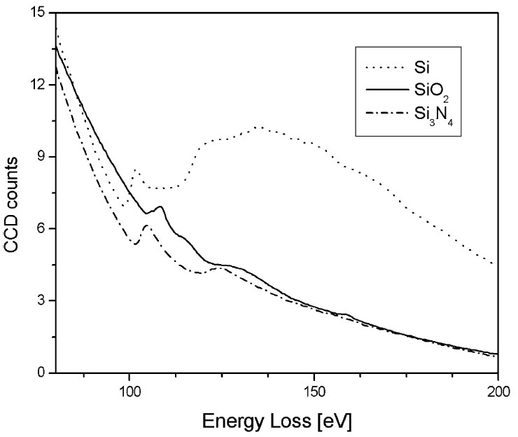
Figure 3391a. Si L2,3 EEL spectra of Si, SiO2 and Si3N4. [1]
In order to distinguish different compounds containing a specific element, e.g. silicon in pure Si, SiO2 and Si3N4, the positions of the energy windows (in three-window method) and respective slit widths have to be chosen according to the ELNES as mentioned above. Table 3391a shows the optimized imaging filter settings in three-window EFTEM mode for Si, SiO2 and Si3N4. For Si mapping in SiO2 the post-edge window was placed above the second peak at 143 eV (See Table 3391a). The two pre-edge windows were placed in the small plateau region between the first (110 eV) and the second (125 eV) peaks. The optimal slit width was found to be 5 eV. The filter settings for Si3N4 were determined in a similar way by considering the shift of the Si L2,3 spectrum towards lower energy loss energies. Therefore the pre-edge windows were placed at 107 and 110 eV. The post-edge window was placed at 114 eV in order to avoid interference with Si and SiO2 signals. A slit width of 3 eV was used. Those settings were used to take Si images in a MOSFET structure as shown in Figure 3391b. Note that in those images, SiO2 and Si3N4 can be distinguished without mapping O and N elements. It is clearly shown that the polycrystalline Si gate (a) is separated by a thin dielectric layer (b) from the single crystalline Si (c). The spacers (d) consisting of two different types of material can be seen on both sides of the gate. Between the polycrystalline gate and the single crystalline Si, the gate oxide layer is also seen clearly. The spacers consist of two layers, namely a thin SiO2 layer and a thicker Si3N4 layer. Note that the bright contrast at the top of image (c) can be an artifact because of the signal of some elements overlapping the Si energy windows of SiO2.
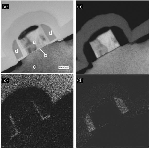
Figure 3391b. TEM bright field image and ELNES Si maps of the MOSFET structure: (a) TEM bright field image; (b) Si map; (c) Si map in SiO2; (d) Si map in Si3N4.
[1]
Table 3391a. The imaging filter settings of EFTEM for Si, SiO2 and Si3N4. [1]
| Compound |
Pre-edge window 1 (eV) |
Pre-edge window 2 (eV) |
Post-edge window (eV) |
Slit width (eV) |
Si |
73 |
87 |
119 |
20 |
SiO2 |
110 |
125 |
143 |
5 |
Si3N4 |
107 |
110 |
114 |
3 |
The valence state of Co can be indirectly determined by mapping the Si ELNES characteristics for the cases of CoSix (x = 1 or 2). Figure 3391c shows the as-measured and background-subtracted Si L2,3 EELS spectra of CoSi and CoSi2. The spectra for both silicides have Si L2,3 edge onsets located at 100.6 eV, while the Si ELNESs are slightly different. The CoSi2 ELNES has one broad peak with a characteristic pre-edge peak, while the CoSi ELNES does not show this pre-edge peak. Based on those characteristics, the parameters for three-window EFTEM method in Table 3391b are used. Here, in order to distinguish between CoSi and CoSi2, the pre-edge peak of CoSi2 was used, while the third peak of CoSi at 145 eV was used for the post-edge window. Using those settings, the Si ELNES maps of CoSi and CoSi2 were obtained together with TEM image as shown in Figure 3391d. Note that the Ti, Co, and Si elements had overlapped layers as indicated in Figure 3391d (a). Although the Ti film also gave some artefacts in the maps, it is very important that the grains consisting of CoSi and CoSi2 were still distinguished and the images revealed that a CoSi2 layer was formed between CoSi and Si substrate.
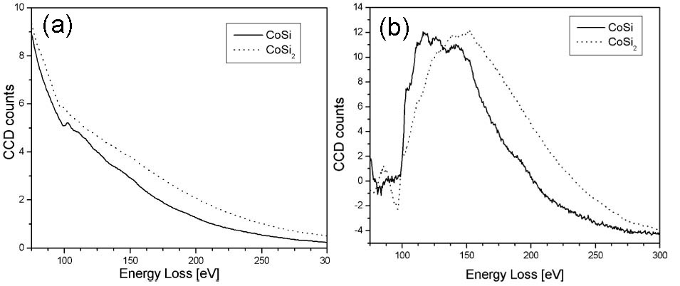
Figure 3391c. The as-measured (a), and background-subtracted (b) Si L2,3 EELS spectra of CoSi and CoSi2. Adapted from [1]
Table 3391b. Three-windows imaging filter settings for Si L2,3 ELNES for CoSi and CoSi2. [1]
| Compound |
Pre-edge window 1 (eV) |
Pre-edge window 2 (eV) |
Post-edge window (eV) |
Slit width (eV) |
CoSi |
125 |
130 |
145 |
10 |
CoSi2 |
67 |
77 |
91 |
6 |
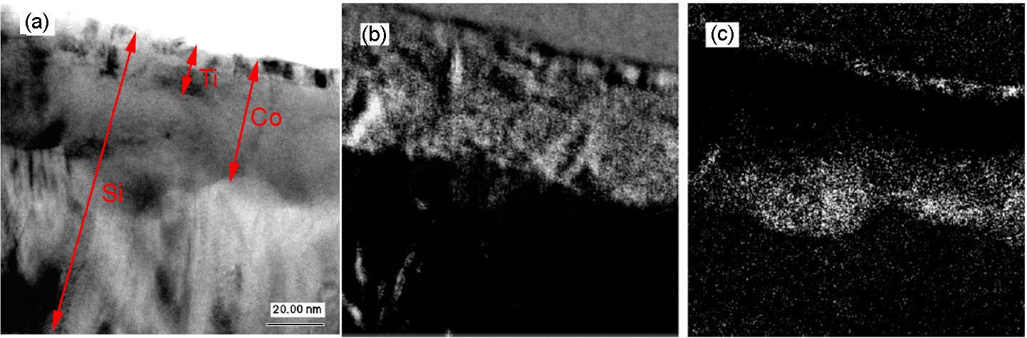
Figure 3391d. The TEM image (a), CoSi map (b), and CoSi2 map (c) of Ti/CoSi/CoSi2 layer stack. Adapted from [1].
[1] M. Worch, H.J. Engelmann, W. Blum, E. Zschech, Cross-sectional thin film characterization of Si compounds in semiconductor device structures using both elemental and ELNES mapping by EFTEM, Thin Solid Films 405 (2002) 198–204.
|