Chapter/Index: Introduction | A | B | C | D | E | F | G | H | I | J | K | L | M | N | O | P | Q | R | S | T | U | V | W | X | Y | Z | Appendix
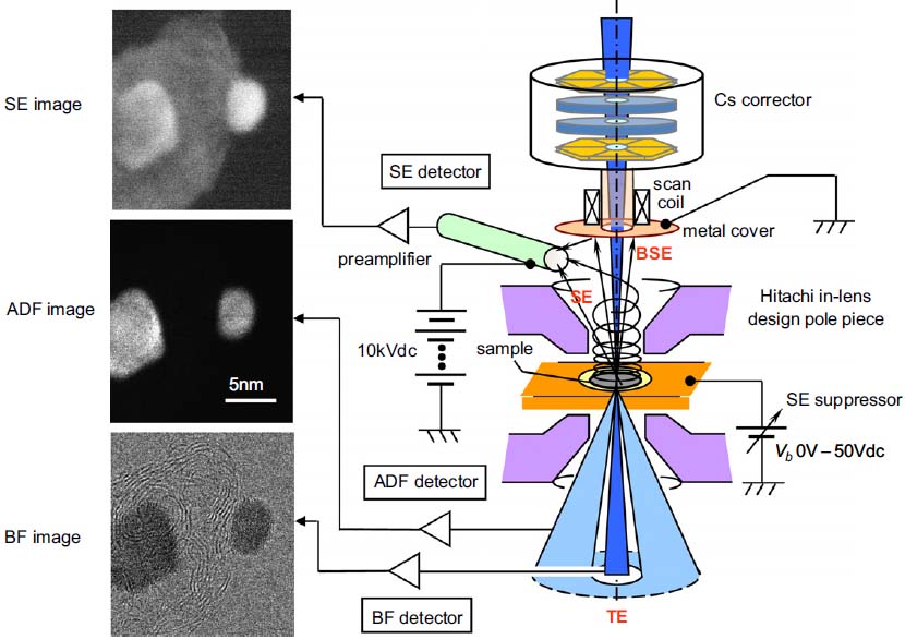
| Most modern scanning electron microscopes (SEMs) can record surface morphology but does not provide atomic resolution. The first atomic resolution, Hitachi aberration-corrected electron microscope, HD-2700C (Figure 4444a) was installed at Brookhaven National Laboratory [1]. This microscope has a pole piece similar to the `in-lens' design used in the S-5500SEM, and has SEM, BSE, and high-angle annular dark-field (ADF) detectors. Later on, Inada, Zhu, et al. [2] in the same group reported detailed investigation of high-resolution imaging using secondary electrons (SE) with a sub-nanometer (~0.1) probe in the same aberration-corrected transmission electron microscope. Figure 4444a shows the schematic illustration of HD 2700C electron microscope which can be used to simultaneously record SE (secondary electron) image using SE and backscattered electrons (BSE), bright- field (BF) STEM image using transmitted electrons (TE) scattered in the forward direction, and annular dark-field (ADF) STEM image using transmitted electrons scattered at large angles. The three images were obtained from Pd/C catalysts in the same area of the carbon support. It can be seen that the BF, ADF, and SE images are complementary. Furthermore, the positive bias of 10 kV in the Hitachi SE detector above the sample is applied to collect low-energy electrons generated at the surface of the specimen for ultrahigh-resolution SE imaging. The positive electric bias of 50 eV on the specimen can suppress the escape of the SEs (with ≤ 50 eV) from the surface, but allow the backscattered electrons with higher energies reaching the detector.
Figure 4444a. Schematic illustration of HD 2700C electron microscope. [2] Figure 4444b shows HAADF-STEM and SE images of a gold nanoparticle, indicating that Au (111) lattice fringes with a 0.24 nm lattice spacing are visible in both images. However, the signal-to-noise ratio of the HAADF-STEM image is much greater than that of the SEM image. The two images were recorded simultaneously on a Cs-corrected HD-2700 STEM/SEM. The accelerating voltage and the probe size were 200 kV and 0.1 nm, respectively. Note that only few cases with successful lattice observations in SEMs had been reported up to date because of the strict sample quality and crystal orientation. Therefore, such work, especially for industry, may be neither time-efficient nor cost-efficient.
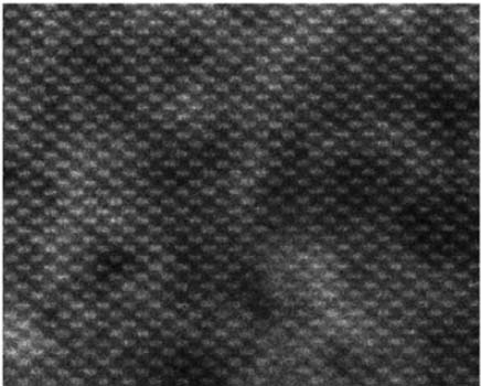
Figure 4444b. (a) HAADF-STEM and (b) SE images of a gold nanoparticle, indicating Au(111) lattice fringes. [3] Inada and Zhu, et al. [2] obtained high-resolution secondary electron microscopy (HRSEM) images of silicon (Si) TEM specimens along (110) direction, taken in a HD 2700C electron microscope using a 0.1 nm scanning probe with a Cs corrector. Figure 4444c shows the lattice fringes of a HRSEM image taken from a TEM specimen covered with a 3 nm amorphous layer induced by FIB specimen preparation. The speckle contrast is due to variation in thickness of the 3-nm amorphous layer. They also found visible lattice fringes in very low intensity for a specimen with an amorphous Si layer of 8 nm thick, while there was only a little atomic contrast in the (110) lattice for a specimen with an amorphous Si layer of 28 nm thick.
Figure 4444c. HRSEM image of a Si TEM specimen along (110) direction. Adapted from [2]
[1] Y. Zhu, H. Inada, K. Nakamura, and J. Wall, Imaging single atoms using secondary electrons with an aberration-corrected electron microscope, Nature Materials, 8 (2009) 808.
|