| For some materials (especially wide band gap materials), the band gap (Eg) from low-loss spectra obtained by EELS technique can be determined by eye observation of the SSD (single scattering distribution) spectrum. In this case, Eg is defined as the energy corresponding to the first onset in the spectrum, for instance, 0.67 and 1.12 eV for Ge and Si respectively, in the schematic spectra in Figure 2406a.
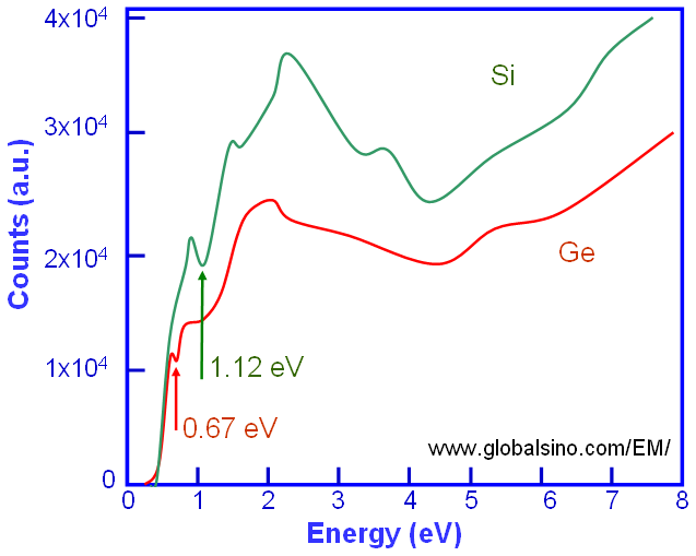
Figure 2406a. Schematic illustration of Si and Ge SSD spectra in the low-energy range.
On the other hand, the band gap can also be determined based on Bethe’s theory. In this case, the SSD spectrum is described to be proportional to the product of the joint density of states (JDOS). Here, the JDOS is given by (e.g. Figure 2406b),
 for a direct band gap, ------------- [2406a] for a direct band gap, ------------- [2406a]
and,
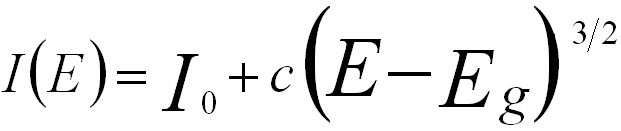 for an indirect band gap ------------- [2406b] for an indirect band gap ------------- [2406b]
where,
I0 and c -- The constants.
E -- The energy loss.
| Figure 2406b. EELS intensity recorded from cubic GaN by using a monochromated TEM-EELS system, presenting direct and indirect electronic transitions. [14] |
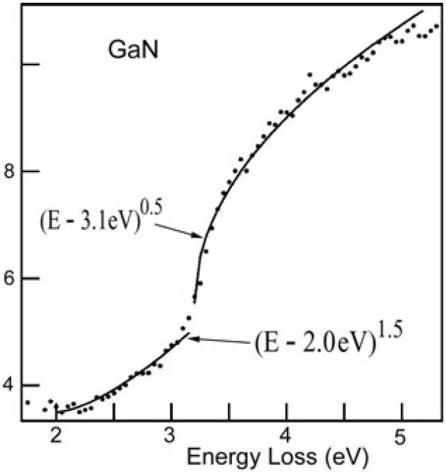
Therefore, Eg can be extracted by fitting the single scattering spectrum using Equations [2406a] and [2406b].
Figure 2406c shows the band gap determination of the HfO2 layer in a Si/SiO2/HfO2/poly-Ge stack by using Equation 2406a (direct band gap [Eg = 5.26 eV] for HfO2).
| Figure 2406c. Band gap determination of the HfO2 layer in a Si/SiO2/HfO2/poly-Ge stack. Adapted from [1] |
However, at very low energy losses, especially in the range of 0 to 5 eV, the current deconvolution methods for multiple inelastic scattering are not sufficiently accurate [2]. For instance, in this energy range, any differences between the experimental and modelled zero-loss peaks (ZLPs) can create large, random data spikes in the deconvoluted spectrum.
As shown above, several methods have been applied to determine the band gap from low-loss spectra in EELS technique. [3-7] However, such technique is not widely used for band gap measurements because of the presence of “parasitic” unwanted losses which are superimposed to the band gap signal. Fortunately, according to the simulations based on the so-called Kröger formula [17], all the unwanted losses, with only a small momentum transfer, happen at very low scattering angles and can, in general, be avoided by not using the scattering events in that small scattering range (in ~ μrad range) [11, 18]. That is, there is a large difference in scattering angles between the interband and “parasitic” signals so that the evaluation of band gap can be improved with a carefully chosen angular range to collect the electrons scattered away from the forward direction. [15, 16]
| Table 2406a. Suggested solution of avoiding unwanted energy losses (in a ~ μrad semi-angle range) in band gap determination with low-loss spectra in EELS technique. |
Factors or artifacts affecting measurement accuracy |
Solution |
Reference |
Unwanted losses through the emission of Cherenkov radiation or the excitation of surface-guided light modes |
Minimized by using an annular or off-axis
collection aperture |
[11] |
| Minimized by subtracting spectra recorded with small and large collection
apertures |
[11] |
| Subtracted spectra recorded
with two different collection angles |
[13] |
Zero-loss peak |
|
|
Zero-loss peak tails extended to several eV |
Minimized with a monochromator |
[10, 12] |
| Minimized by setting the parallel-recording spectrometer to a high enough energy dispersion (low
eV/channel) |
[10] |
| Remove the high-energy tail by fitting and subtraction or by Fourier ratio deconvolution |
[11] |
Band gap (Eg) position |
Obtained with the intersection point of linear fits to the intensity rise and
background, e.g. Figure 2406d. |
[12] |
Band gap mapping limited by delocalization of inelastic scattering |
|
|
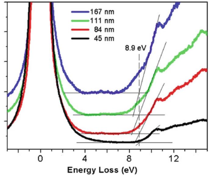
Figure 2406d. Bandgap
measurements on SiO2 (silicon
oxide) films of different
thicknesses. The band gap
(8.9 eV) was obtained with the intersection of linear fits to the intensity rise and
background. [12] |
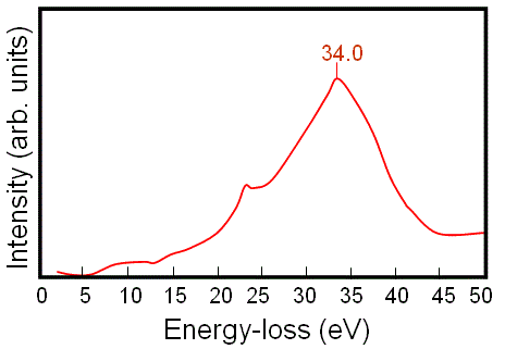
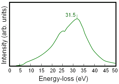
It is very general that the band gap is determined based on Kramers-Kronig analysis. For instance, Figure 2406e shows the EEL spectra of plasmon region (zero-peak is not shown) for crystalline and amorphous diamond. The loss function (Im[-l/ε]) can then be obtained by removing contribution from multiple scattering using the Fourier-log deconvolution method.
Figure 2406e. EEL spectra of plasmon region for (a) crystalline and (b) amorphous diamond.
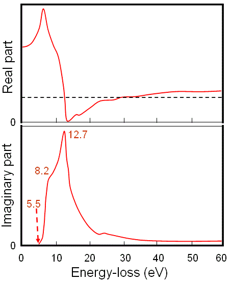
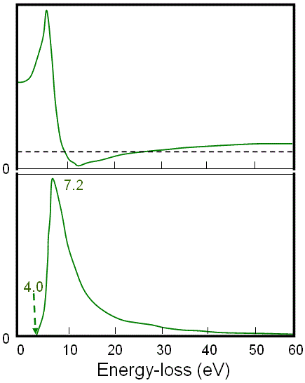
An optical absorption method can directly provide the imaginary part of the dielectric function, ε2, associated with a single electron excitation of an interband transition, while EELS cannot directly give ε2. Based on the obtained loss function, the real part (ε1), and the imaginary part (ε2) of the dielectric function for the crystalline and the amorphous diamond are extracted using Kramers-Kronig analysis as shown in Figure 2406f. Table 2406b lists the onset energy (indicating the band gap energy) and the peaks in the imaginary spectrum obtained from Figure 2406f and the original interband transitions.
| Figure 2406f. Real part (ε1), and the imaginary part (ε2) of the dielectric function for (a) crystalline and (b) amorphous diamond. |
| Table 2406b. Onset energies (band gap energies), peaks in the imaginary spectrum in Figure 2406f and the original interband transitions. |
| |
Onset energy (band gap energy) |
Peaks in imaginary spectrum |
Interband transition |
Crystal diamond |
5.5 eV |
8.2 |
Γ point |
| 12.7 |
X and L points |
Amorphous diamond |
4.0 eV |
7.2 eV |
Γ point |
[1] Marie C. Cheynet, Simone Pokrant, Frans D. Tichelaar, and Jean-Luc Rouvière, Crystal structure and band gap determination of HfO2 thin films, Journal of Applied Physics 101, 054101 (2007).
[2] U. Bangert and R. Barnes. Electron energy loss spectroscopy of defects in diamond. Phys. Stat. Sol. (A), 204 (7): 2201–2210, 2007.
[3] A. Gutiérrez-Sosa, U. Bangert, A.J. Harvey, C.J. Fall, R. Jones, P.R. Briddon, M.I. Heggie, Band-gap-related energies of threading dislocations and quantum wells in group-III nitride films as derived from electron energy loss spectroscopy, Phys. Rev. B - Condens. Matter Mater. Phys. 66 (2002) 353021–3530210. doi:10.1103/PhysRevB.66.035302.
[4] H. Lakner, B. Rafferty, G. Brockt, Electronic structure analysis of (In,Ga,Al)N heterostructures on the nanometre scale using EELS, J. Microsc. 194 (1999) 79–83.
[5] P.E. Batson, K.L. Kavanagh, J.M. Woodall, J.W. Mayer, Electron-energy-loss scattering near a single misfit dislocation at the GaAs/GaInAs interface, Phys. Rev. Lett. 57 (1986) 2729–2732. doi:10.1103/PhysRevLett.57.2729.
[6] S. Lazar, G.A. Botton, M.Y. Wu, F.D. Tichelaar, H.W. Zandbergen, Materials science applications of HREELS in near edge structure analysis and low-energy loss spectroscopy, Ultramicroscopy. 96 (2003) 535–546. doi:10.1016/S0304-3991(03)00114-1.
[7] Svetlana Korneychuk, Bart Partoens, Giulio Guzzinati, Rajesh Ramaneti, Joff Derluyn, Ken Haenen, Jo Verbeeck, Exploring possibilities of band gap measurement with off-axis EELS in TEM, 189, 2018, 76-84.
[8] P.A. Cherenkov, Visible emission of clean liquids by action of γ radiation, Dokl. Akad. Nauk USSR. 2 (1934).
[9] S.I. Vavilov, On the possible causes of blue γ-glow of liquids, Dokl. Akad. Nauk USSR. 2 (1934).
[10] Bangert, U., Harvey, A. J., Fruendt, D., and Keyse, R., Highly spatially resolved electron
energy-loss spectroscoy in the bandgap region of GaN. J. Microsc. 188, 237–242, (1997).
[11] Stöger-Pollach, M., Optical properties and bandgaps from low loss EELS: Pitfalls and
solutions. Micron 39, 1092–1110, (2008).
[12] Park, J., and Yang, M., Determination of complex dielectric functions at HfO2/Si interface
by using STEM-VEELS. Micron 40, 365–369, (2009).
[13] Zhang, L., Erni, R., Verbeek, J., and Van Tenderloo, G. (2008) Retrieving the dielectric function of
diamond from valence electron energy-loss spectroscopy. Phys. Rev. B 77, 195119 (7 pages).
[14] Lazar, S., Botton, G. A., Wu, M.-Y., Tichelaar, F. D., and Zandbergen, H. W. (2003) Materials science
applications of HREELS in near edge structure analysis and low-energy loss spectroscopy.
Ultramicroscopy 96, 535–546.
[15] Korneychuk, S.; Partoens, B.; Guzzinati, G.; Ramaneti, R.; Derluyn, J.; Haenen, K.; Verbeeck, J. Exploring possibilities of band gap measurement with off-axis EELS in TEM. Ultramicroscopy 2018, 189, 76–84.
[16] Stöger-Pollach, M.; Schachinger, T.; Biedermann, K.; Beyer, V. Valence EELS below the limit of inelastic delocalization using conical dark field EFTEM or Bessel beams. Ultramicroscopy 2017, 173, 24–30.
[17] E. Kröger, Transition radiation Cerenkov radiation and energy losses of relativistic charged particles traversing thin foils at oblique incidence, Zeitschrift F. Phys. (1970) 403–421.
[18] L. Zhang, Electron energy loss spectroscopy Fundamental aspects and its application to diamond, PhD Thesis, University of Antwerp, 2010.
|