|
|
Smallest Structures Obtained by Dual Beam SEM/FIB/STEM Deposition
- Practical Electron Microscopy and Database -
- An Online Book -
|
|
https://www.globalsino.com/EM/
|
|
This book (Practical Electron Microscopy and Database) is a reference for TEM and SEM students, operators, engineers, technicians, managers, and researchers.
|
=================================================================================
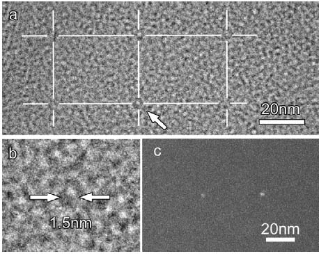
Electron-beam-induced deposition (EBID) has normally been performed in scanning electron microscopes (SEMs). In this case, the smallest deposited structures depend on the distribution of secondary electrons rather than primary electrons [3]. Therefore, the smallest structures that are obtainable in EBID are 15–20 nm in size, determined by the spreading profile of the secondary electrons. However, researchers had recently attempted to minimize the secondary-electron effect by using a field-emission (FE) STEM. For instance, Mitsuishi et al. [1] successfully fabricated nanodots with 3.5 nm in diameter by using an intense electron beam in a 200 keV FE-STEM. In this case, the size of the deposited dots does not depend on the substrate thickness. Furthermore, Tanaka et al. [2] had successfully fabricated W (tungsten) nanodots with EBID in an ultrahigh-vacuum FE-TEM (UHV-FE-TEM). The size of the dots depended on the pressure in the chamber. The smallest particle size obtained was about 1.5 nm in diameter as shown in Figure 2484.

Figure 2484. Array of the smallest W nanodots formed by EBID: (a) TEM image of an array, (b) Magnified TEM image of a dot indicated by the arrow in (a), and (c) corresponding HAADF-STEM (Z-contrast) images. [2]
[1] Mitsuishi K, Shimojo M, Han M and Furuya K 2003 Appl.
Phys. Lett. 83 2064.
[2] Tanaka M, Shimojo M, Han M, Mitsuishi K and Furuya K 2005 Surf. Int. Anal. 37 261.
[3] Kohlmann-von Platen K T, Chiebek J, Weiss M, Reimer K,
Oertel H and Brunger W H 1993 J. Vac. Sci. Technol. B
11 2219.
|
=================================================================================
The book author (Yougui Liao) welcomes your comments, suggestions, and corrections, please click here for submission. If you let book author know once you have cited this book, the brief information of your publication will appear on the “Times Cited” page.
|
|
