=================================================================================
In STEM mode, each element of the electron source can be assumed to emit electrons incoherently and thus results in an incoherent broadening of the probe [5]. Atomic number- (Z-) contrast imaging can provide qualitative and quantitative two-dimensional (2-D) information on the chemical composition. Such images are obtained by the detection of elastically and quasi-elastically scattered electrons using a high-angle annular dark-field (HAADF) detector. To form Z-contrast images, the STEM objective aperture must be inserted to cut out high-angle electron rays, and an annular detector must be inserted after the projector lens system.
As discussed in page 2579, a collection angle higher than 50 mrad allows acquisition of mainly incoherent electrons in the HAADF image [1]. In general, these radii of ADF detector for Z-contrast can both vary over a large range from lab to lab; however,
typically the inner radius would be in the range of 30–100 mrad and
the outer radius 100–200 mrad. Lakner et al. used angular range between 60 and 180 mrad for mapping structure of GaAs/GaInP semiconductor heterostructures. They suggested that scattering in this range is dominated by Rutherford (elastic) scattering and thermal diffuse (quasi-elastically) scattering (TDS). Note that TDS was previously considered as “background intensity”. In HAADF imaging, such high-angle scattering is very sensitive to the atomic number (Z) of the scattering atoms and therefore provides information of the local chemical composition [2]. In many applications, we can consider the high angle scattering follows Rutherford’s law only, i.e. the scattering cross section is proportional to effective scattering potential or to Zε(g) (ε = 1.2~ 2) [7-11] (see Cross-Section at page4667). As shown in Figure 4788a, the larger the inner angle (with larger g), the closer ε approaches to the value 2, which is
the classical Rutherford scattering result for an unscreened nucleus. Therefore, the Z-dependence of the ADF signal could be improved significantly by increasing the inner collection angle of the ADF detector.
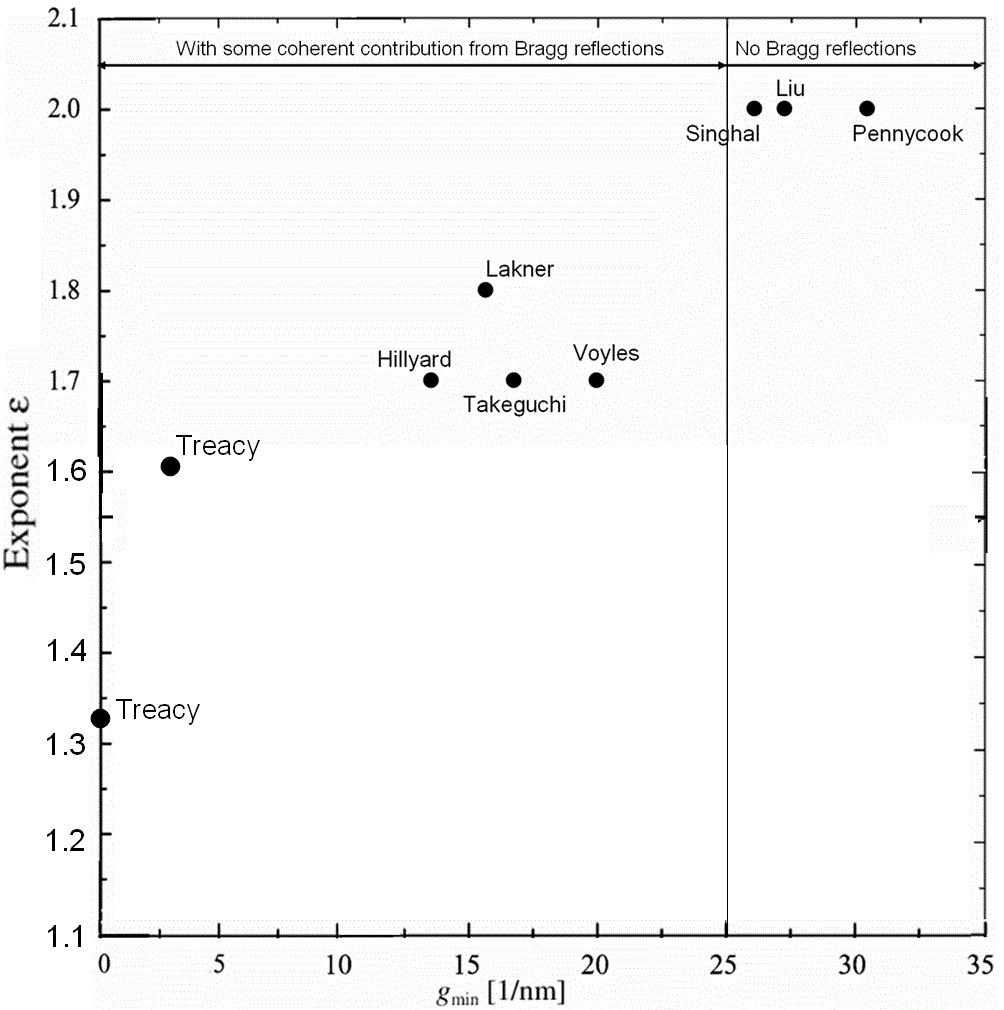
| Figure 4788a. Exponent versus annular detector inner collection vectors. [17-24] The collection vectors can be converted to collection angles for different accelerating voltages, for instance, the 25 nm-1 corresponds to ~100 mrad at 100 kV. (see page1196) |
The physical mechanism for this Z-dependent behavior is that high-angle scattering is mostly from the electrons scattered by the inner cores of atoms. The partial screening of the atomic nucleus by the inner shell electronic charges is responsible for the value of n to be less than 2 for a pure Rutherford scattering. Z-contrast technique has further been used for high-resolution STEM (HRSTEM) imaging. In this case, the use of a HAADF-STEM signal removes the complexity of conventional bright-field scattering in HRTEM and the associated diffraction complications and the incoherent images are directly interpretable. However, in many cases the purity of Z-contrast in HAADF images is still a question (See page2582).
Due to its unique performances, ADF-STEM has been applied in many fields:
i) Identification of the presence of nanostructures with high signal-to-noise ratio. For instance, the empty space or carbon film on Cu grid represents as ‘dark area’ in the images and nanostructures present bright dots.
ii) Elemental identification of amorphous materials based on Z-contrast theory.
iii) Elemental identification in crystals based on Z-contrast theory if all the elements are in the same crystal structure (e.g. page1245).
Figure 4788b (a) shows a HAADF-STEM image of single-layered h-BN (hexagonal boron-nitride) and Figure 4788b (b) is a corresponding atomic model where a EELS linescan has been recorded, shown in (c) and (d). The STEM contrast of the N and B locations is determined by the atomic number, called Z-contrast. Figure 4788b (c) and (d) shows the EELS profiles of the boron K-edge and nitrogen K-edge signals, respectively.
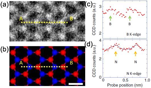
| Figure 4788b. (a) A HAADF-STEM image of single-layered h-BN (hexagonal boron-nitride), (b) A corresponding atomic model where a EELS linescan was recorded, and (c) and (d) the EELS profiles of the boron K-edge and nitrogen K-edge signals. Adapted from [4] |
In Figure 4788c, the intensities of the Nb and Ni atom columns in [010] direction shows the -Ni-Nb-Nb- ordering in Ba3NiNb2O9 in P-3m1 (164) space group. Its lattice parameters are a = b = 5.7550(5) Å and c = 7.0656(2) Å.
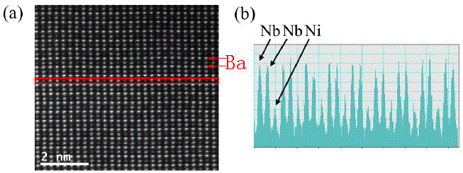
| Figure 4788c. HAADF intensities of the Nb and Ni atom columns in [010] direction showing the -Ni-Nb-Nb- ordering. Brightest contrast: Ba (Z=88); brighter contrast: Nb (Z = 73); weak contrast: Ni (Z=46). [14] |
Generally speaking, the formation of bright-field and dark-field TEM/STEM images normally obeys the principle of the monotonic increase of cross sections σ(Z) for thermal diffuse, elastic, and inelastic scatterings. For instance, the high-angle scattered electrons in HAADF measurements are predominantly those electrons which have undergone thermal scattering. Therefore, if there is no diffraction effects, darker (lighter) contrasts in bright-field (dark-field) images, respectively, are associated with heavier elements, for instance, as shown in Figure 4788d for a Pt/Cr interface with ZCr = 24 and ZPt=78.
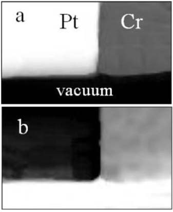
Figure 4788d. Contrasts of Pt/Cr interface in dark-field (a) and bright-field (b) TEM/STEM images. Adapted from [6]
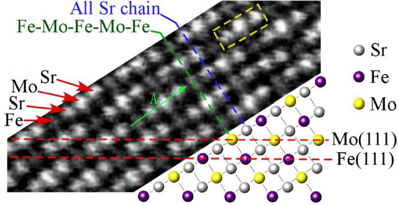
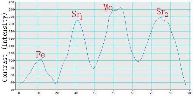
Some other factors can also affect the HAADF contrast of the atoms. For many complex compounds, one need to carefully select the observation direction for HAADF-STEM imaging in order to correctly analyze the Z-contrast of different elements with closer atomic numbers. In such cases, they need to first study the crystalline structure with simulators to figure out the crystal orientation in which each atomic column contains a single type of elements only. The number of atoms in a single atomic column may also need to be taken into account. For instance, the observation of <1-10> direction for double perovskite (DP) Sr2FeMoO6 structures is a good choice. Figure 4788e (a) presents an HAADF-STEM observation of elemental ordering in a DP Sr2FeMoO6 film and a schematic projection drawing of the lattice along the <1-10> direction. Each lattice site becomes a column of pure Sr (Z=38), Fe (Z=26), or Mo (Z=42) atoms, respectively, and thus each site gives its unique brightness in the HAADF-STEM image, originated from their atomic numbers. The bright Sr-Mo-Sr triplets separated by a darker Fe atom. Table 4788a list the comparison between the theoretical Z-contrast and experimental intensity. We can know that the ratios of the normalized intensities of Sr and Mo atoms are slightly greater than the ratios of their normalized Z-contrast factors (Z1.7). For Sr atom columns, their intensity is not constant and they have an intensity variation of about 5%, which is in the range of common systematic errors. In this experiment, an aberration-corrected HAADF STEM system in a FEI Titan TEM is operated at 300 kV. The specimen thickness is ~50 nm and the specimen preparation was finalized by Argon (Ar) milling.
 |
 |
| (a) |
(b) |
Figure 4788e. (a) HAADF-STEM image and schematic projection drawing of the DP Sr2FeMoO6 lattice along the <1-10> direction. Each triplet is a bright Sr-Mo-Sr chain (e.g. the dashed yellow box). Adapted from [16]. And (b) Brightness (intensity) plot of a Fe-Sr-Mo-Sr chain along the green arrow in (a). |
Table 4788a. Comparison between the theoretical Z-contrast and experimental intensity.
| Elements |
Atomic number (Z) |
Theoretical Z1.7 |
Normalized Z1.7 |
Experimental intensity |
Normalized intensity |
| Fe |
26 |
254.4 |
1.00 |
107 |
1.00 |
| Sr1 |
38 |
484.9 |
1.91 |
212 |
1.98 |
| Mo |
42 |
574.8 |
2.26 |
246 |
2.30 |
| Sr2 |
38 |
484.9 |
1.91 |
222 |
2.07 |
In Figure 4788f, multislice simulation presents the total cross section of Au (gold) as a function of the number of atoms in a Au column.[12] In other words, the HAADF intensity depends on the atomic number (Z-contrast) as well as the number of atoms in the column. Without the need for a calibration standard, LeBeau et al. [13] were able to quantify the number and location of the atoms in the specimen from 4 to 33 atom column height when the experimental images taken from a wedge-shaped Au thin foil was compared directly with theory.
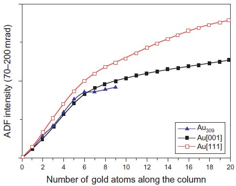
Figure 4788f. HAADF intensity as a function of the number of atoms along the Au column, obtained by multislice simulation. [12]
Table 4788b lists some examples of elemental groups which had been studied by researchers and had been suggested whether the elements are experimentally distinguishable within each group by HAADF technique. Assuming ZA > ZB, in general, the elements can be distinguished at atomic scale if A1.7/B1.7 > 5 with very thin specimens, and the elemental layers can be separated at low magnifications of 2 < A1.7/B1.7 < 5 (e.g. Nb/Ni) with "thick" specimens. The elements cannot be distinguished at all at any magnifications if A1.7/B1.7 < 2. However, for a well-aberration-corrected HAADF STEM, the distinguishability is much greater, e.g. one even was able to seperate the Mo and Sr atom columns (Mo1.7/Sr1.7=1.19).
Table 4788b. Examples of elemental groups studied by researchers.
| Group |
Symbol |
Elements |
Atomic number (Z) |
Z1.7 |
A1.7/B1.7 |
Distinguishability |
Reference |
| 1 |
A |
Sb |
51 |
799.6 |
9.0 |
Yes |
[3]; also see page1245 |
| B |
Si |
14 |
88.8 |
| 2 |
A |
Cr |
78 |
1,646.5 |
7.4 |
Yes |
[6]; also see Figure 4788d |
| B |
Pt |
24 |
222.0 |
| 3 |
A |
Ni/Cu |
28/29 |
~288.5 |
3.69 |
Yes |
[15]; also see Al87Ni7Cu3Ce3 in page1437 |
| B |
Al |
13 |
78.29 |
| 4 |
A |
Ce |
58 |
995.0 |
~3.45 |
Yes |
[15]; also see Al87Ni7Cu3Ce3 in page1437 |
| B |
Ni/Cu |
28/29 |
~288.5 |
| 5 |
A |
Nb |
73 |
1,471.1 |
2.2 |
Yes |
[14]; also see Figure 4788c |
| B |
Ni |
46 |
670.9 |
| 6 |
A |
Y |
39 |
506.8 |
1.6 |
Not |
[15] |
| B |
Zn |
30 |
324.4 |
| 7 |
A |
Mo |
42 |
574.8 |
1.19 |
Yes |
[16]; also see Figure 4788e or Table 4788a (with aberration-correction) |
| B |
Sr |
38 |
484.9 |
| 8 |
A |
Cu |
29 |
306.3 |
~1.06 |
Not |
|
| B |
Ni |
28 |
288.5 |
| 9 |
|
O |
8 |
34.3 |
|
Invisible by HAADF |
|
Note that the Z-contrast principle will break down for thick specimens above a certain thickness, due to multiple scattering of electrons, which depends on the specimen material, accelerating voltage and collection semi-angle.
Table 4788c. Thickness dependence of validation of Z-contrast principle in AADF imaging.
Specimen thickness |
Validation of Z-contrast principle |
Thick |
Not valid |
Thin |
Valid |
Low angle -ADF |
Not valid |
High angle-ADF |
Valid |
Table 4788d.
Visibility of elements with HAADF technique.
| 1 |
2 |
|
3 |
4 |
5 |
6 |
7 |
8 |
9 |
10 |
11 |
12 |
13 |
14 |
15 |
16 |
17 |
18 |
| 1 |
|
2 |
| H |
|
He |
| 3 |
4 |
|
5 |
6 |
7 |
8 |
9 |
10 |
| Li |
Be |
| Green: Visible |
Red: invisible |
|
|
|
B |
C |
N |
O |
F |
Ne |
| 11 |
12 |
|
13 |
14 |
15 |
16 |
17 |
18 |
| Na |
Mg |
|
Al |
Si |
P |
S |
Cl |
Ar |
| 19 |
20 |
|
21 |
22 |
23 |
24 |
25 |
26 |
27 |
28 |
29 |
30 |
31 |
32 |
33 |
34 |
35 |
36 |
| K |
Ca |
|
Sc |
Ti |
V |
Cr |
Mn |
Fe |
Co |
Ni |
Cu |
Zn |
Ga |
Ge |
As |
Se |
Br |
Kr |
| 37 |
38 |
|
39 |
40 |
41 |
42 |
43 |
44 |
45 |
46 |
47 |
48 |
49 |
50 |
51 |
52 |
53 |
54 |
| Rb |
Sr |
|
Y |
Zr |
Nb |
Mo |
Tc |
Ru |
Rh |
Pd |
Ag |
Cd |
In |
Sn |
Sb |
Te |
I |
Xe |
| 55 |
56 |
|
71 |
72 |
73 |
74 |
75 |
76 |
77 |
78 |
79 |
80 |
81 |
82 |
83 |
84 |
85 |
86 |
| Cs |
Ba |
{57-70} |
Lu |
Hf |
Ta |
W |
Re |
Os |
Ir |
Pt |
Au |
Hg |
Tl |
Pb |
Bi |
Po |
At |
Rn |
| 87 |
88 |
|
103 |
104 |
105 |
106 |
107 |
108 |
109 |
110 |
111 |
112 |
|
114 |
| Fr |
Ra |
[89-102] |
Lr |
Rf |
Db |
Sg |
Bh |
Hs |
Mt |
Ds |
Uuu |
Uub |
|
Uuq |
| |
|
57 |
58 |
59 |
60 |
61 |
62 |
63 |
64 |
65 |
66 |
67 |
68 |
69 |
70 |
|
|
| {lanthanides} {57-70} |
La |
Ce |
Pr |
Nd |
Pm |
Sm |
Eu |
Gd |
Tb |
Dy |
Ho |
Er |
Th |
Yb |
|
|
|
89 |
90 |
91 |
92 |
93 |
94 |
95 |
96 |
97 |
98 |
99 |
100 |
101 |
102 |
|
|
| {actinides} [89-102] |
Ac |
Th |
Pa |
U |
Np |
Pu |
Am |
Cm |
Bk |
Cf |
Es |
Fm |
Md |
No |
|
|
| |
[1] M. M. J. Treacy, A. Howie, and S. J. Pennycook, Inst. Phys. Conf. Ser. 52, 261 (1980).
[2] Characterization of III–V semiconductor interfaces by Z -contrast imaging, EELS and CBED, Hubert Lakner, Bernd Bollig, Stefan Ungerechts and Erich Kubalek, J. Phys. D: Appl. Phys. 29 1767–1778 (1996).
[3] P. M. Voyles, D. A. Muller, J. L. Grazul, P. H. Citrin, and H.-J. L. Gossmann, Atomic-scale imaging of individual dopant atoms and clusters in highly n-type bulk Si, Nature, 416 (2002) 826.
[4] Kazu Suenaga, Haruka Kobayashi, and Masanori Koshino, Core-Level Spectroscopy of Point Defects in Single Layer h-BN, Physical Review Letters, 108, 075501 (2012).
[5] J.M. Cowley, Image contrast in transmission scanning
electron microscopy, Appl. Phys. Lett. 15 (1969) 58-60.
[6] Konstantin Iakoubovskii, Kazutaka Mitsuishi,Yoshiko Nakayama, and Kazuo Furuya, Mean free path of inelastic electron scattering in elemental solids and oxides using transmission electron microscopy: Atomic number dependent oscillatory behavior, Physical Review B 77, 104102 (2008).
[7] Bals S., Kilaas R. and Kisielowski C., Ultramicroscopy 104 (2005) 281.
[8] P. Hartel, H. Rose, C. Dinges, Ultramicroscopy 63 (1996) 93–114.
[9] Krivanek OL, Chisholm MF, Nicolosi V, Pennycook TJ, Corbin GJ, Dellby N, et al. Nature,
2010;464:571–4.
[10] Hartel P. Ultramicroscopy 1996;63:93–114.
[11] Wang Z, Li ZY, Park S, Abdela A, Tang D, Palmer RE. Phys Rev B 2011;84:073408.
[12] Jiang J. Structural characterization and investigation of the growth mechanism for the pentacle
nanowires. PhD Thesis, Tsinghua University, 2009.
[13] LeBeau JM, Findlay SD, Allen LJ, Stemmer S. Nano Lett 2010;10:4405–8.
[14] Jungmin Hwang, Magnetoelectric and Multiferroic Properties in Layered 3d Transition Metal Oxides, thesis, 2012.
[15] Eiji Abe, Atomic-Scale Characterization of Nanostructured Metallic Materials by HAADF/Z-contrast STEM, Materials Transactions, 44(10), 2035-2041, (2003).
[16] Adam Joseph Hauser, Unlocking the potential of half-metallic Sr2FeMoO6 thin films through controlled stoichiometry and double perovskite ordering, PhD thesis, 2010.
[17] Michael M.J. Treacy, Z Dependence of Electron Scattering by Single Atoms into Annular Dark-Field Detectors, Microsc. Microanal. 17, 847–858, 2011, doi:10.1017/S1431927611012074.
[18] Hillyard S and Silcox J 1995 Ultramicroscopy 58, 6.
[19] Lakner H, Mendorf C, Bollig B, Prost W and Tegude FJ 1997 Mat. Sci. Eng. B 44, 52.
[20] Liu CP, Twesten RD and Gibson JM 2001 Ultramicroscopy 87, 79.
[21] Pennycook SJ, Rafferty B and Nellist PD 2000 Microsc. Microanal. 6, 343.
[22] Signhal A, Yang JC and Gibson JM 1997 Ultramicroscopy 67, 191.
[23] Takeguchi M, McCartney MR and Smith DJ 2004 Appl. Phys. Lett. 84, 2103.
[24] Voyles PM, Grazul JL and Muller DA 2003 Ultramicroscopy 96, 251.
|