EELS Measurements of Oxygen (O) - Practical Electron Microscopy and Database - - An Online Book - |
|||||||||||||||||||||||||||||
| Microanalysis | EM Book http://www.globalsino.com/EM/ | |||||||||||||||||||||||||||||
Table 3392a lists the O edge that is used in EELS analysis. It is well-known that background subtraction of the O edge in the presence of Ti (due to its L2,3 edge at ~455 eV) is very challenging. In general, using a energy window in the range of 467 - 527 eV gives the most consistent results in terms of power law background subtraction. Table 3392a. O edge used in EELS analysis.
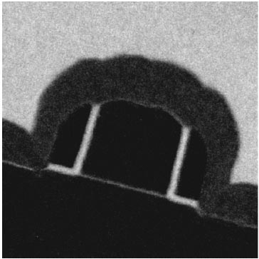
Figure 3392a shows oxygen (O) map of MOSFET structure taken by an energy filter in EFTEM. The bright areas show O element, while the gray and dark areas were from other materials, such as Si3N4, silicon (Si) substrate, and polycrystalline Si.
Figure 3392a. O map of MOSFET structure taken by an energy filter. [1]
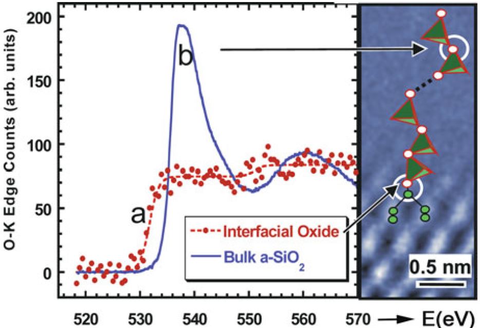
Figure 5.55 shows how the background-subtracted oxygen K-edge changed
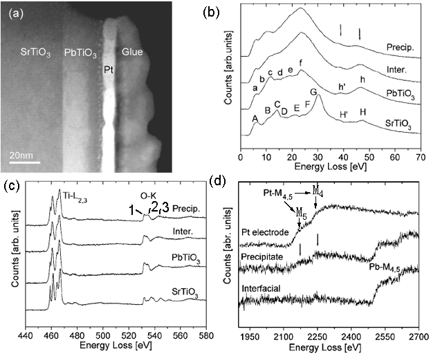
The sandwich structure shown in Figure 3392c (a) is composed of three layers: SrTiO3, PbTiO3, and Pt. An amorphous Ti-rich interfacial layer as well as nanometer size precipitates was formed at PbTiO3/Pt interfaces. In the low-loss region in EELS from the different layers shown in Figure 3392c (b), the energy peaks labeled A–H for SrTiO3 and a–h for PbTiO3 are formed by interband transitions which are typical in bulk SrTiO3 and PbTiO3 [2]. The strong peaks H/h and H’/h’ arise from transitions of Ti 3p to higher energy levels such as Ti 3d, Ti 4s, forming Ti M2,3 edge. In the precipitates, the transitions h and h are reduced in intensity because these precipitates might be Ti-deficient. In Figure 3392c (c), the two core loss EELS profiles from SrTiO3 and PbTiO3 layers show clear splitting of the Ti-L2,3 edges, while for the interfacial layer the splitting at the Ti-L3 edge is much less and the splitting at the Ti-L2 edge disappears. The splitting of Ti-L2,3 edges reflects the hybridization and ligand field strength of Ti–O atomic interaction so that the reduction of splitting in the interfacial layer reflects the weaker Ti–O bonding force. Due to the similar hybridization of O 2p states with Ti 3d in the conduction band, the energy region from 530 eV to 536 eV is split into two subbands t2g (marked peak 1) and eg (marked peak 2). Figure 3392c (d) shows the EEL spectra of Pb- and Pt-M4,5 edges.
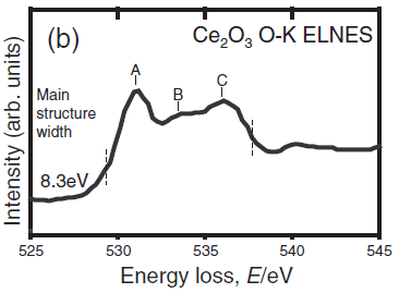
In most cases, EELS measurement on Ce2O3 can be unsuccessful because of the rapid oxidation of the sample during its transfer into the TEM system. [5] Figure 3392d shows the measured O-K ELNES without such oxidation. The main structure width, including the three broad peaks A, B and C, was evaluated as the distance between the positions of the broken lines corresponding to the minimum and maximum in the second differentiated spectra.
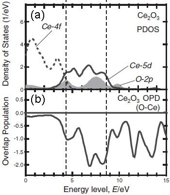
Figure 3392d. The measured O-K ELNES. [6] Figure 3392e shows the unoccupied partial density of states (PDOS) of Ce2O3 and the bond overlap population diagram (BOPD) between Ce and its neighboring O for the non-core-holed, ground state electronic structures. The main peak structures of the ELNES in Figure 3392d correspond to the Ce5d derived states, which range from 3 to 9 eV above the Fermi level (the Fermi level in Figure 3392e is set to zero). Since the intensities of the BOPD are negative, the corresponding interactions between the Ce and anion O atoms are all antibonding. Larger BOPD intensities correspond to larger spatial overlaps between the two molecular orbitals, promoting higher antibonding energy levels. [7] The spatial overlaps between the Ce5d and the O orbitals show a variation in the Ce5d-derived states, resulting in the energy width of Ce5d PDOS and the main peak structures in the ELNES in Figure 3392d.
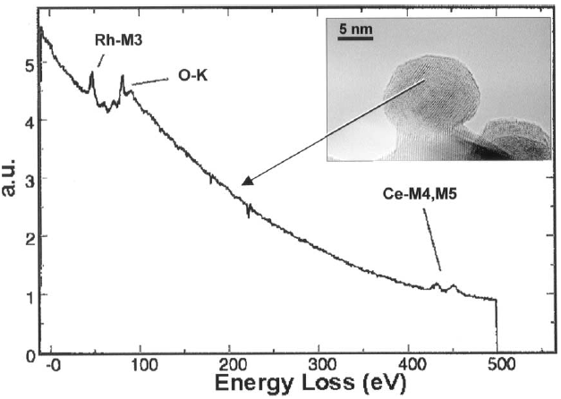
Figure 3392f shows an EEL spectrum recorded in spot mode inside a catalytic particle, presenting Rh-M3, O-K, and Ce-M4,M5 white lines.
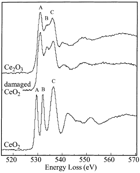
Figure 3392f. EEL spectrum presenting Rh-M3, O-K, and Ce-M4,M5 white lines. [4] Figure 3392g shows the comparison of the O K-edges of CeO2, Ce2O3, and electron beam damaged CeO2. The energy-loss near-edge structure (ELNES) of the beam-damaged CeO2 presents O K-edge shapes that are consistent with reduction to a Ce3+ oxide (Ce2O3). Table 3392b also lists the energies of the EELS peaks of the two oxides and their formation mechanisms.
Figure 3392g. Comparison of the O K-edges of CeO2, Ce2O3, and electron beam damaged CeO2. [11]
Table 3392b. The EELS peaks of two oxides and their formation mechanisms.
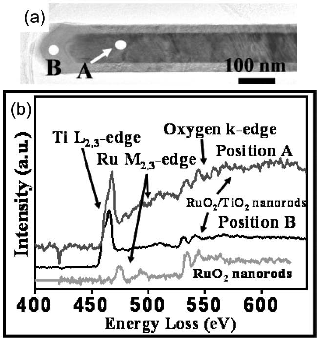
Figure 3392h (a) shows a TEM image of a RuO2/TiO2 core/shell structure (a RuO2 nanorod shelled with a TiO2 layer) in diameter of 160 nm. Figure 3392h (b) shows the EELS spectra taken from the selected positions in Figure 3392h (a) that are marked by A and B for the RuO2/TiO2 core/shell structure and a pure RuO2 nanorod without TiO2 coating, respectively. For the EEL spectrum from the TiO2 shell (position B), the ELNESs of Ti L2,3- and O K-edges are clearly found. In the spectrum obtained from position A, the Ru M-edge is present, while the Ti L2,3- and O K-edges are not so clear (comparing to noise) because the wire-shaped specimen is too thick (about 220 nm in wire-diameter) for EELS measurements.
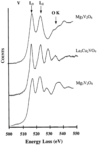
In the determination of the stoichiometry of the vanadate oxides, the researchers have mainly focused on the high energy loss regions, including the vanadium L2,3 peaks and oxygen K peak, for instance shown in Figure 3392i. The vanadium L2 and L3 peaks denote electronic transitions from vanadium 2p1/2 and 2p3/2 states to the orbitals with 3d state [14]. The oxygen k-edge (between 525 and 550 eV) presents the transition from the oxygen 1s state to the orbitals with oxygen 2p state. Note that care is needed when we are doing mapping analysis or quantification, e.g. using three-window method, since the V edges and O edge are very close in energy.
Figure 3392i. EEL spectra: (a) Mg3V2O6, (b) La3Cu2VO9 and (c) Mg3V2O8. [13]
[1] M. Worch, H.J. Engelmann, W. Blum, E. Zschech, Cross-sectional thin film characterization of Si compounds in semiconductor device structures using both elemental and ELNES mapping by EFTEM, Thin Solid Films 405 (2002) 198–204. |
|
||||||||||||||||||||||||||||