Chapter/Index: Introduction | A | B | C | D | E | F | G | H | I | J | K | L | M | N | O | P | Q | R | S | T | U | V | W | X | Y | Z | Appendix
| Table 3508a. Main edges of Ti used in EELS analysis.
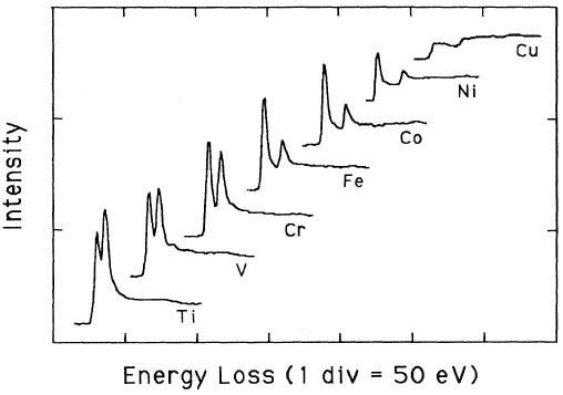
Pearson et al. [3] experimentally and theoretically (based on one-electron Hartree-Slater calculations) found that the intensities of L2,3 white lines for most of the 3d and 4d transition metals decreased nearly linearly with increasing atomic number, reflecting the filling of the d states. Figure 3508a shows the deconvoluted and background-subtracted L2,3 energy-loss spectra for the 3d transition metals. The edge energies are not shown in order to present all the spectra in the same figure, while the intensities of the white lines are scaled simultaneously for all elements.
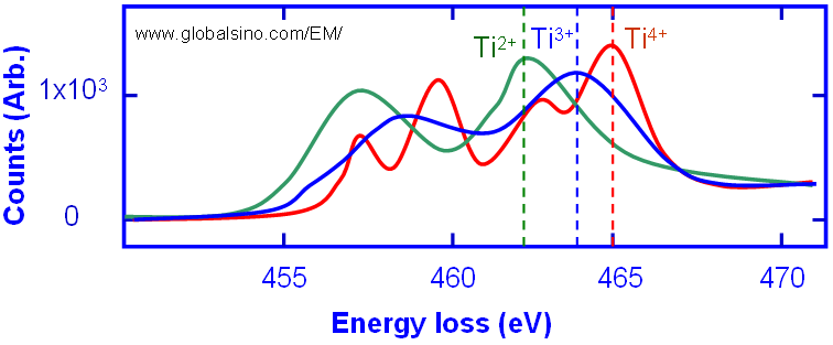
The Ti L2,3 near-edge structures in EELS spectrum for Ti2+, Ti3+ and Ti4+ are different as shown in Figure 3508b, indicating a lower oxidation state has L2,3 edges shift slightly towards the lower energy loss. Here, the green curve shows the fine structure of Ti2+ state, the blue curve the fine structure of Ti3+ state, and the red curve the fine structure of Ti4+ state.
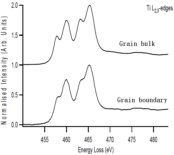
Figure 3508b. The Ti L2,3 near-edge structures in EELS spectrum for Ti2+, Ti3+, and Ti4+. Figure 3508c compares the EELS profiles taken from a grain boundary and a grain bulk of perovskite-type CaCu3Ti4O12 (with grain sizes of 100-300 µm). Based on HRTEM imaging, it was suggested that the grain boundary exhibited a step-like morphology and high local stress due to the change of chemistry and/or structure. The bulk EEL data suggested that Ti is presented as Ti4+, while the EEL data for the grain boundary suggested that Ti had a trivalent component.
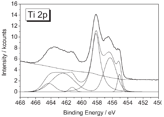
For comparison purpose, Figure 3508d shows the Ti 2p XPS profile of a native TiN layer.
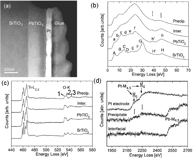
Figure 3508d. The Ti 2p XPS profile of a native TiN layer. [4] This ionic decomposition of Ti is probably the consequence of three effects: i) The octahedral symmetry of the Ti sites in TiO6 is preserved (for SrTiO3 and LaTiO3); ii) The extra electron resides on the Ti site; and iii) The Ti 2p–3d–3d couplings in the presence of the core hole are large than the dispersion widths of the 3d bands [1 - 2]. The sandwich structure shown in Figure 3508e (a) is composed of three layers: SrTiO3, PbTiO3, and Pt. An amorphous Ti-rich interfacial layer as well as nanometer size precipitates was formed at PbTiO3/Pt interfaces. In the low-loss region in EELS from the different layers shown in Figure 3508e (b), the energy peaks labeled A–H for SrTiO3 and a–h for PbTiO3 are formed by interband transitions which are typical in bulk SrTiO3 and PbTiO3 [5]. The strong peaks H/h and H’/h’ arise from transitions of Ti 3p to higher energy levels such as Ti 3d, Ti 4s, forming Ti M2,3 edge. In the precipitates, the transitions h and h are reduced in intensity because these precipitates might be Ti-deficient. In Figure 3508e (c), the two core loss EELS profiles from SrTiO3 and PbTiO3 layers show clear splitting of the Ti-L2,3 edges, while for the interfacial layer the splitting at the Ti-L3 edge is much less and the splitting at the Ti-L2 edge disappears. The splitting of Ti-L2,3 edges reflects the hybridization and ligand field strength of Ti–O atomic interaction so that the reduction of splitting in the interfacial layer reflects the weaker Ti–O bonding force. Due to the similar hybridization of O 2p states with Ti 3d in the conduction band, the energy region from 530 eV to 536 eV is split into two subbands t2g (marked peak 1) and eg (marked peak 2). Figure 3508e (d) shows the EEL spectra of Pb- and Pt-M4,5 edges.
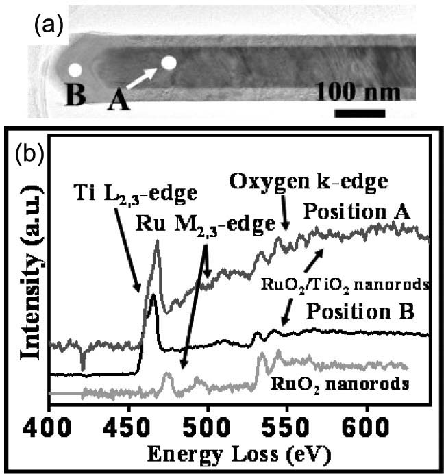
Figure 3508f (a) shows a TEM image of a RuO2/TiO2 core/shell structure (a RuO2 nanorod shelled with a TiO2 layer) in diameter of 160 nm. Figure 3508f (b) shows the EELS spectra taken from the selected positions in Figure 3508f (a) that are marked by A and B for the RuO2/TiO2 core/shell structure and a pure RuO2 nanorod without TiO2 coating, respectively. For the EEL spectrum from the TiO2 shell (position B), the ELNESs of Ti L2,3- and O K-edges are clearly found. In the spectrum obtained from position A, the Ru M-edge is present, while the Ti L2,3- and O K-edges are not so clear because the wire-shaped specimen is too thick (about 220 nm in wire-diameter) for EELS measurements.
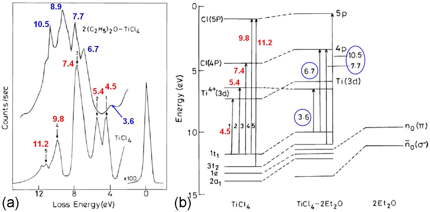
Figure 3508g shows the EELS recorded with a home-built spectrometer [7], and the energy level diagram and electronic transitions of TiCl4 and TiCl4-2Et2O complex. For TiCl4, there are five prominent peaks 1 to 5 (in red). The first peak at 4.5 eV originates from the transition 1t1 to e, while the second one at 5.4 eV is due to the transition 1t1 to 1t2. The intense peak at 7.4 eV originates from the Rydberg transition 1t1 to 4P. The features at 9.8 and 11.2 eV originate from the transitions from the 1t1 and 3t2 orbitals to the Cl(5P) level. The spectrum of the TiCl4-2Et2O complex has the transitions at 3.6, 6.7, 7.7, 8.9, and 10.5 eV (in blue). The first peak at 3.6 eV originates from the charge transfer band due to the transition from the highest occupied shifted chlorine lone pair orbital to the Ti4+(3d). The peaks at 6.7 and 7.7 eV are from the transitions from the shifted 1t1 and 3t2 chlorine orbitals to the 4p Rydberg states. This shift is due to the complex formation. The peak at 10.5 eV originates from the 3t2 to 5p transition. Therefore, when the tetrahedral TiCl4 molecule is bonded to form octahedral TiCl4-2Et2O, the molecule should become more ionic. [8] The charge-transfer band in TiCl4 at 4.5 eV is shifted to 3.6 eV because of the change in the electronic structure of the molecule.
The experimental ELNES spectra at the Ti-L2,3 edge taken from amorphous, C49, and C54 TiSi2 are very similar.
[1] Yu-Lun Chueh, Chin-Hua Hsieh, Mu-Tung Chang, Li-Jen Chou, Chang S. Lao, Jin H. Song, Jon-Yiew Gan, and Zhong L. Wang, RuO2 Nanowires and RuO2/TiO2 Core/Shell Nanowires: From Synthesis to Mechanical, Optical, Electrical, and Photoconductive Properties, Advanced Materials, 2007, 19 (1), 143–149.
|