Chapter/Index: Introduction | A | B | C | D | E | F | G | H | I | J | K | L | M | N | O | P | Q | R | S | T | U | V | W | X | Y | Z | Appendix
| In general, the TEM samples that are too thin have too few atoms to produce sufficient signals to generate statistical reliability. However, the TEM samples also cannot be too thick for any measurements. The best balance is normally determined experimentally. The list in Table 4487a presents empirical thicknesses for the EELS, EFTEM, EDS, and HAADF STEM measurements. Table 4487a. Empirical thicknesses for EELS, EFTEM, EDS, and HAADF STEM measurements*.
As we know that in TEM observation, the transmission of unscattered incident electrons is inversely proportional to the TEM specimen thickness. On the other hand, the increase of the specimen thickness enhances the energy loss of the transmitted electrons. Therefore, the spatial resolution degrades with the increase of specimen thickness because of the chromatic aberration effects. EELS measures the distribution of energies lost by incident electrons (typically 100–1000 keV) as they pass through a thin solid specimen (typically 0.5–50 nm). Table 4487b lists examples of the energy loss of incident electrons passing through the specimen. The use of thinner specimen can generally improve spatial resolution because it minimizes the energy loss. Table 4487b. Examples of the energy loss of electrons passing through the TEM specimen.
The interpretation of data and images taken from TEM systems can be very complicated if there is a variation of specimen thickness. Especially, for quantitative composition analysis of electron energy loss spectroscopy (EELS) measurements, energy filtered TEM (EFTEM) images, and high angle annular dark field scanning TEM (HAADF STEM) images, a uniform or exactly known sample thickness is preferable because the recorded signal intensity depends strongly on both sample thickness and sample composition. If the TEM specimen is very thick, both the chromatic and spherical aberrations affect the spatial resolution of EFTEM imaging significantly. For instance, for thick specimen the chromatic broadening (Δdc) is about 2.5 nm at β = 10 mrad, Cc = 1 mm, ΔE = 50 eV, and E0 = 200 keV, while for thin specimen, Δdc will be normally ≤ 0.2 nm for most microscope configurations (see details in page3384). For thick specimen, assuming the spherical aberration constant is 0.7 mm, collection semi-angle 15 mrad, the ΔdS will be ~3.8 nm, while for thin specimen ΔdS is normally negligible for most microscope configurations (see details in page1941). In the cases that very thick TEM samples are used in EELS or EFTEM measurements, the increase of plural scattering effects induces two main problems: On the other hand, if the TEM samples are too thin, either inelastic scattering does not occur or is too weak to do EELS and EFTEM measurement. With a STEM sample thickness less than 50 Å, Voyles et al [1] concluded that ADF-STEM image obtained at 200 kV can show a Si column containing a single Sb atom is more than 25% brighter than a pure Si column. They also suggested that random variations in thickness must be less than the contrast of one Sb atom, and the surfaces must be free from native amorphous SiO2 layers and amorphized bulk Si layers in ADF-STEM observations. Investigating individual point defects, e.g. monovacancies, using TEM-related techniques was believed to be difficult because this requires both atomic sensitivity and atomic resolution and the specimens need to be very thin such that one can detect the individual point defects from the image contrast. Table 4487c. Examples of TEM specimen thicknesses for EELS measurements.
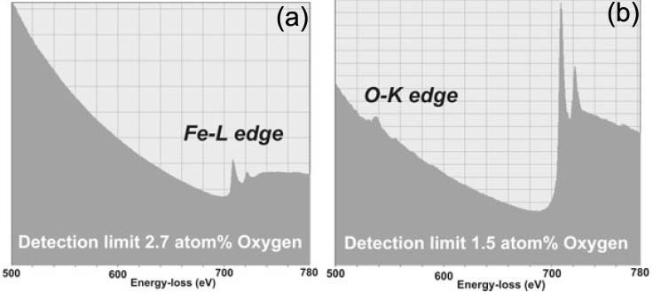
Furthermore, the detection limit is also controlled by the sample thickness because of the background. For instance, the detection limit of oxygen was improved from 2.7 atomic % (130 nm thickness in Figure 4487a (a)) to 1.5 atomic % (40 nm thickness in Figure 4487a (b)), assuming that the minimum detectable counts of oxygen are equal to the 3 sigma of signal/noise ratio under the analytical conditions [3]. Therefore, the oxygen content is not detectable in the 130-nm thick sample because the concentration is lower than the detection limit. Note that the two spectra were taken from the same (Mg, Fe)O-matrix phase.
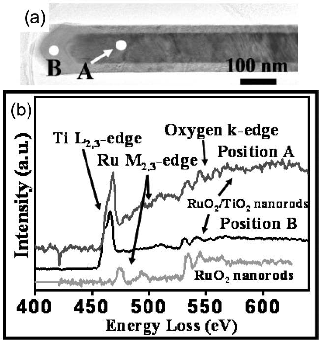
Figure 4487a. Example of thickness dependence of EELS detection limits. The TEM samples are (Mg, Fe)O-matrix phase in thickness of: (a) 130 nm and (b) 40 nm. Adapted from [2] Figure 4487b (a) shows a TEM image of a RuO2/TiO2 core/shell structure (a RuO2 nanorod shelled with a TiO2 layer) in diameter of 160 nm. Figure 4487b (b) shows the EELS spectra taken from the selected positions in Figure 4487b (a) that are marked by A and B for the RuO2/TiO2 core/shell structure and a pure RuO2 nanorod without TiO2 coating, respectively. For the EEL spectrum from the TiO2 shell (position B), the ELNESs of Ti L2,3- and O K-edges are clearly found. In the spectrum obtained from position A, the Ru M-edge is present, while the Ti L2,3- and O K-edges are not so clear (comparing to noise) because the wire-shaped specimen is too thick (about 220 nm in wire-diameter) for EELS measurements, even though the EELS contribution of TiO2 thickness (about 60 nm, including top and bottom TiO2 layers of the nanorod) is almost the same as that at location B and the O atomic percentage is high (about 67 at.%).
Figure 4487b. (a). The TEM image of a RuO2/TiO2 core/shell structure in diameter of 160 nm. (b) EELS spectrum for the Ti L-edge and O K-edge ELNEFS of the RuO2/TiO2 core/shell structure taken from two points, labeled A and B for the RuO2/TiO2 wire and the TiO2 shell, respectively. The bottom EELS spectrum was obtained from a pure RuO2 nanorod as reference. Adapted from [5] Furthermore, the spatial resolution of STEM measurements is also determined by the specimen thickness, due to cone shape of the probe. For instance, if we have the experimental conditions below: For very thin TEM specimens, e.g. ≤30 nm for Si (or ≤0.25 λP), several surface-induced effects contribute to plasmon signal: In general, the requirements of TEM specimen thickness for EELS and EFTEM measurements are: A common measurement for selecting appropriate sample thickness is to test the ratio of the count of the zero-loss peak, I0, to that of the first plamon peak, Ip. A number of values have been suggested for the maximum acceptable Ip/I0 ratio, range form 1 to 0.1 depending on the chemistry of the analyzing materials. It is not possible to give a reliable general value for an acceptable Ip/I0 ratio. However, it is evident that a strong zero-loss peak is an important feature for a usable specimen thickness. The maximum usable specimen thickness can be increased by Note that for high resolution STEM analysis, very thin high-quality TEM specimens are needed as discussed in page2939.
[1] P. M. Voyles, D. A. Muller, J. L. Grazul, P. H. Citrin, and H.-J. L. Gossmann, Atomic-scale imaging of individual dopant atoms and clusters in highly n-type bulk Si, Nature, 416 (2002) 826.
|
||||||||||||||||||||||||||||||||||||||||||||