=================================================================================
Reducing the accelerating voltage of the electron beams in EMs, e.g. STEM and TEM, helps to avoid beam damage in specimens but will degrade the spatial resolution and/or the contrast of the images. For instance, in low-voltage STEM mode, reducing the acceleration voltage requires increase of the convergence semi-angle in order to form the electron probe to maintain a constant radius of the Airy disc induced by the diffraction limit.
Therefore, it is necessary to compensate for geometrical aberrations up to higher convergence semi-angles at low acceleration voltages. Fortunately, some efforts can be performed to compensate for these negative effects. For instance, a TEM/STEM system equipped with a cold field emission gun and spherical aberration correctors for image- and probe-forming systems can still have high spatial resolution to resolve the lattice fringes of materials such as Si, Ge, and Au crystals even though working at very low accelerating voltages in the range of 30 to 60 kV [1]. In this case, a delta-type aberration corrector was designed to simultaneously compensate for third-order spherical aberration (C3,0) and fifth-order 6-fold astigmatism (C5,6).
Figure 2235a shows the photograph of a LVEM (low-voltage electron microscope) with delta Cs correctors operated in the range 30 - 60 kV. The CFEG stands for cold field emission gun installed on the top of the column. The delta correctors for STEM and TEM are integrated for both probe- and image-forming systems. An Enfina spectrometer is installed at the bottom of the column for EELS-based measurements.
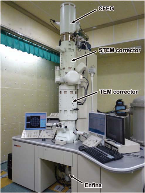
Figure 2235a. The photograph of a LVEM with delta Cs correctors operated in the range 30 - 60 kV. [1]
Figures 2235b (a) and (c) show HAADF images of Si [110] taken in a Cs-corrected STEM system at 30 kV and 60 kV, respectively. Si (silicon) dumbbells, in which two Si columns are separated by 136 pm, are clearly shown in both cases. In Figure 2235b (b), the Fourier transform of the HAADF image (a) contains a clear -224 spot (corresponding to the lattice spacing of 111 pm), while in Figure 2235b (d), the Fourier transform of the HAADF image (c) shows clear -115 and -440 spots (corresponding to the lattice spacings of 105 and 96 pm, respectively).
![HAADF images of Si [110] taken at 30 kV and 60 kV](image1/2235b.jpg)
Figure 2235b. (a) and (c) HAADF images of Si [110] taken at 30 kV and 60 kV, respectively, and (c) and (d) The Fourier transform of the HAADF image (a) and (b).
[1]
Using the same Cs corrected system shown in Figure 2235a, Sasaki et al. [1] were also able to record high resolution TEM (HRTEM) images of gold (Au) nanoparticles at the accelerating voltages of 30 and 60 kV.
[1] Takeo Sasaki, Hidetaka Sawada, Fumio Hosokawa, Yuji Kohno, Takeshi Tomita, Toshikatsu Kaneyama, Yukihito Kondo, Koji Kimoto, Yuta Sato, and Kazu Suenaga, Performance of low-voltage STEM/TEM with delta corrector and cold field emission gun, Journal of Electron Microscopy 59(Supplement): S7–S13 (2010).
|