Dependence of EELS Signal on TEM Specimen Thickness - Practical Electron Microscopy and Database - - An Online Book - |
||||||||
| Microanalysis | EM Book https://www.globalsino.com/EM/ | ||||||||
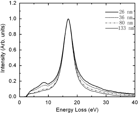
Mkhoyan et al. [1] presented SSDs (single scattering distributions) obtained from experimental EELS data from silicon (Si) specimens with four different thicknesses as shown in Figure 2401a. The band gap or electronic states in the gap presented in the figure were inaccurate due to the low energy-resolution. In their measurements, the energy resolution was 0.7 eV, and the channel size 0.22 eV so that it was impossible to quantify features located below 2 eV.
Figure 2401a. SSDs obtained from experimental EELS data from Si specimens with four different thicknesses.
Adapted from [1]
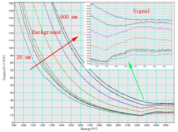
Note that the surface plasmon-loss (Is) has dependence on TEM-specimen thickness only when the specimen is extremely thin (e.g. <10 nm in general). On the other hand, for very thin TEM specimens, e.g. ≤30 nm for Si (≤0.25 λP), several surface-induced effects contribute to plasmon signal: In general, the requirements of TEM specimen thickness for EELS and EFTEM measurements are: Figure 2401b shows that the background increases dramatically with increase of the thickness of TEM specimen, while the signal of Pt M4,5 edge decreases significantly. The highest signal in the range of these TEM specimen thicknesses for Pt occurs at 20 nm.
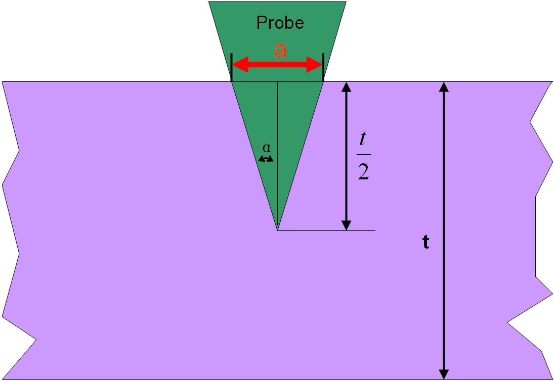
Figure 2401b. EELS of Pt M4,5 edge. Furthermore, the "local" EELS intensity also depends on the spatial resolution of STEM. However, the spatial resolution of the measurements in STEM mode can be estimated by the diameter of the probe irradiation on the specimen. Assuming the thickness of the specimen is t, then the spatial resolution is given by (see Figure 2401c):
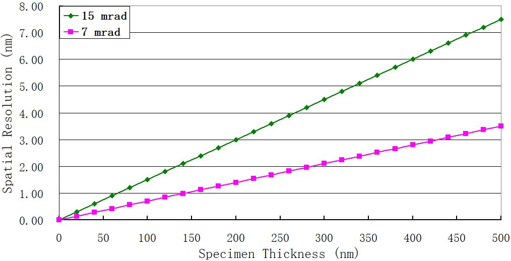
For instance, Figure 2401d shows the spatial resolutions at convergence semiangles 7 and 15 mrad, respectively, based on Equation 2401. Note that such convergence semiangles are used in many TEM systems.
[1] K.A. Mkhoyan, T. Babinec, S.E. Maccagnano, E.J. Kirkland, and J. Silcox, Separation of bulk and surface-losses in low-loss EELS
|
|
|||||||