| The collection semi-angle (β, sometimes called collection angle) is the maximal
scattering semi-angle that is accepted by the EELS (Electron Energy Loss Spectroscopy). In general, β should be 2 - 3 times the characteristic or mostprobable
scattering angle for specific loss processes and β is affected by
your choice of EELS or GIF operating mode. The details of calculation on collection semi-angle in TEM diffraction and STEM mode are described at page4938.
As shown in Table 4941, in a dedicated STEM, β
is determined by the size of the objective aperture, whereas α (convergence semi-angle, sometimes called convergence angle) is determined by
the size of the collection aperture. The semi-convergence is directly proportional to the size of the C2 aperture. For instance, when the C2 aperture is changed from 50 µm to 100 µm, the semi-convergence angle is doubled.
Note that the objective aperture determines
the angular range of illumination of the TEM specimen, whereas the collection aperture is
used to limit the angle of the scattered electrons entering the EELS spectrometer.
In TEM and in normal STEM systems with postspecimen
lenses the situation is more complicated because the postspecimen lenses have the property of changing beam angles. In TEM systems, one has further to distinguish between image mode (image on fluorescent screen) and diffraction mode (diffraction pattern on fluorescent screen). Table 4941 shows how to determine α and β by the apertures in the STEM and TEM.
Table 4941. Aperture factors affecting α and β.
| |
Dedicated STEM |
Image Mode in TEM |
Diffraction Mode in TEM |
| α |
Objective aperture |
Condenser aperture |
Condenser aperture |
| β |
Condenser aperture |
Objective aperture |
The smaller of selected area and objective aperture |
The last condenser lens (Condenser 3 lens for JEOL systems) changes the convergence angle of the illumination as shown in Figure 4941a.
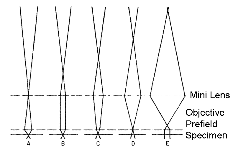
Figure 4941a. Effect of changing the last condenser lens in the electron microscope (EM) system.
In STEM operation, to observe the Ronchigram, the apertures after the specimen are removed and a large probe convergence angle (>100 mrad) is selected, for instance by inserting the largest STEM objective aperture (condenser aperture in CTEM).
In practice, various convergence semi-angles are used by different labs based on the reality of their TEM/STEM systems and the users' preference as shown in Table 4941. The user can find the semi-convergence angle of the probe in the operation interface in some systems. The default semi-convergence of 10-15 mrad is optimum for most systems without probe Cs-corrector.
Table 4941. Examples of convergence semi-angles of STEM systems.
| Convergence semi-angles |
Analyzed materials |
Note |
Reference |
| < 1 mrad |
|
Nearly parallel beam for nano beam diffraction |
[16] |
2 mrad |
Biological materials |
Specimen thickness of 1 µm |
[4] |
| 1-5 mrad |
|
Convergent Beam Electron Diffraction (CBED) |
[10] |
| 2 - 15 mrad |
Typical |
|
[7, 8] |
| 4 - 20 mrad |
|
HAADF applications |
[19] |
| 9 mrad |
|
|
[2] |
| 10 mrad |
|
EELS applications at 100 kV |
[12, 17] |
| 10-12 mrad |
Li1.2Mn0.4Fe0.4O2 |
|
[5] |
| 15 mrad |
Most materials |
Providing a spatial resolution of ~ 1.2 Å for a 300 kV electron microscope. |
[9] |
| 18 mrad |
Al0.86Mg0.22Si0.22Ge0.13Cu (at.%) alloy |
EDS applications |
[3, 13] |
| 19 mrad |
|
EELS applications |
[11] |
| 20 mrad |
|
With the correction of spherical aberration |
[2] |
| 21 mrad |
|
EDS applications |
[13] |
| 23 mrad |
|
|
[6] |
| 20.4 mrad |
|
HAADF applications |
[15] |
| 26 mrad |
|
EDS and HAADF applications |
[13, 18] |
| 28 mrad |
|
ABF applications |
[15] |
| 30 mrad |
|
EELS and HAADF applications |
[14] |
| 31.8 mrad |
|
Aberration-corrected Nion UltraSTEM |
[1] |
[1] Huolin L. Xin, Ye Zhu, David A. Muller, Determining On-Axis Crystal Thickness with Quantitative Position-Averaged Incoherent Bright-Field Signal in an Aberration-corrected STEM, Microscopy and Microanalysis, 18, 2012, pp 720-727.
[2] Science of Microscopy, Volume I, edited by P.W. Hawkes, John C.H. Spence, (2008).
[3] 13th International Conference on Aluminum Alloys (ICAA 13), edited by Hasso Weiland, Anthony Rollett, William Cassada.
[4] Transmission Electron Microscopy: Diffraction, Imaging, and Spectrometry edited by C. Barry Carter, David B. Williams, (2016).
[5] Rechargeable Lithium and Lithium Ion Batteries, Vol. 11 (29), edited by M. C. Smart, (2008).
[6] Atomic Scale Characterization and First-Principles Studies of Si3N4 Interfaces, Weronika Walkosz (2011).
[7] Nanocharacterisation, edited by Angus Kirkland, John Hutchison, (2007).
[8] Spectroscopic Methods in Mineralogy and Material Sciences, edited by Grant Henderson, Daniel Neuville, Robert, (2014).
[9] Light Metals 2013,
edited by Barry A. Sadler.
[10] Linear and Chiral Dichroism in the Electron Microscope, edited by Peter Schattschneider, (2011).
[11] Proceedings of the 18th International Conference on Environmental Degradation of Materials in Nuclear Power Systems - Water Reactors, Volume 1, edited by John H Jackson, Denise Paraventi, Michael Wright, (2018).
[12] Electron Energy-Loss Spectroscopy in the Electron Microscope, R.F. Egerton, (1986).
[13] Three Dimensional Chemical Analysis of Nanoparticles Using Energy Dispersive X-ray Spectroscopy, thesis, Thomas Slater (2015).
[14] Control of Radiation Damage in MoS2 by Graphene Encapsulation Recep Zan, Quentin M. Ramasse, Rashid Jalil, Thanasis Georgiou, Ursel Bangert and Konstantin S. Novoselov.
[15] Dan Zhou, Knut Müller-Caspary, Wilfried Sigle, Florian F. Krause, Andreas Rosenauer, Peter A. van Aken, Sample tilt effects on atom column position determination in ABF–STEM imaging, Ultramicroscopy 160 (2016) 110–117.
[16] D. Alloyeau, C. Ricolleau, T. Oikawa, C. Langlois, Y. Le Bouar, A. Loiseau, STEM nanodiffraction technique for structural analysis of CoPt nanoparticles, Ultramicroscopy 108 (2008) 656–662.
[17] R. Aveyard, Z. Zhong, K. J. Batenburg, B. Rieger, Optimizing experimental parameters for the projection requirement in HAADF-STEM tomography, Ultramicroscopy 177 (2017) 84–90.
[18] Daniel Bahena, Nabraj Bhattarai, Ulises Santiago, Alfredo Tlahuice, Arturo Ponce, Stephan B. H. Bach, Bokwon Yoon, Robert L. Whetten, Uzi Landman, and Miguel Jose-Yacaman, STEM Electron Diffraction and High-Resolution Images Used in the Determination of the Crystal Structure of the Au144(SR)60 Cluster, J. Phys. Chem. Lett. 2013, 4, 975−981.
[19] DQuantitative High-Angle Annular Dark Field Scanning Transmission Electron Microscopy for Materials Science, Dissertation, Rumyana V. Petrova, (2006).
.
|
