=================================================================================
In practice, even though the electron source in TEM is never perfectly coherent, the degree of coherence must be so high that the interference fringe pattern with sufficient quality in electron holography measurements can be recorded within a reasonable acquisition time in which the specimen and/or beam drift can be negligible.
Although electron holograms have historically been recorded on photographic films, digital acquisition using CCD cameras is common in modern microscopes.
The basic requirements for off-axis electron holography analysis are:
i) TEM system with a field emission gun (FEG),
ii) Möllenstedt–Düker biprisms.
Most of the microscope manufacturers provide rotatable biprism assemblies,
iii) Wave optical reconstruction software installed on a modern personal computer (PC). For instance, a plug-in called HoloWorks on the interface of Digital-Micrograph (Gatan Company) can be used to process the recorded holograms [1].
It was also suggested that for quantitative analysis, the image wave reconstructed from sideband should be perfectly zero-loss filtered.
[2]
Basic operation procedures of hologram acquisition and analysis:
Warning: The data acquisition on the same TEM specimen can take a day or a couple of days, and the data selection and analysis can be similarly time-consuming.
a) Prepare a proper TEM specimen with an applicable thickness. For electric field study, FIB-prepared specimens can be as thick as ~400 nm because of electrically inactive layer induced by FIB-damage. (for instance, see page4305).
If you are not working on thickness study, you need to have uniform thickness across the interesting region in the TEM specimen; otherwise, thickness artifact will be induced.
b) Select proper lens combinations. For instance, for electric field, dopant, and p-n junction measurements see page4305.
[Note: Lorentz lens or mode is needed to get large area phase mappings of the electron holograms.]
c) Tilt the specimen away from the major zone axes in order to avoid diffraction artifacts.
d) Align the transmission electron microscope (TEM) to a condition which is suitable for high resolution TEM (HRTEM) imaging.
e) Overfocus the condenser lens, and thus the brightest area is in the middle of the beam spot.
f) Shift the biprism filament into the electron beam.
The biprism filament is oriented (for a rotatable biprism) so that the analyzing area in the specimen is located on one side of the filament shadow, while the other side stays empty as a reference area. Note that only a small deviation from the preferred direction of the biprism filament is tolerable at the cost of the interference fringe contrast.
[3]
g) Obtain elliptical illumination using the stigmator controls of the condenser lens (Figure 2603a) [4, 5].
The source has to be extended as far as possible perpendicularly to the biprism filament, while in parallel to the biprism filament, a much smaller extension of the coherent domain is sufficient.
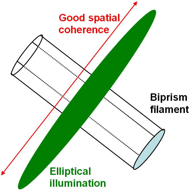
Figure 2603a. Elliptical illumination for optimum contrast. Adapted from [3]
h) Locate the biprism in the middle of the long axis of the elliptical illumination.
i) Increase the voltage UF at the biprism filament so that the shadow of the biprism vanishes and a bright interference region with broad interference fringes is developed. [3]
j) Further perform the perpendicular alignment of the source in respect to the biprism [3]:
j.1. Coarse alignment. The direction of the bright interference region always stays along the biprism filament when the condenser is changed from underfocus to overfocus and vice versa as shown in Figure 2603b.
j.2. Fine alignment. In this step, the interference fringe contrast is focused as shown in Figure 2603c.
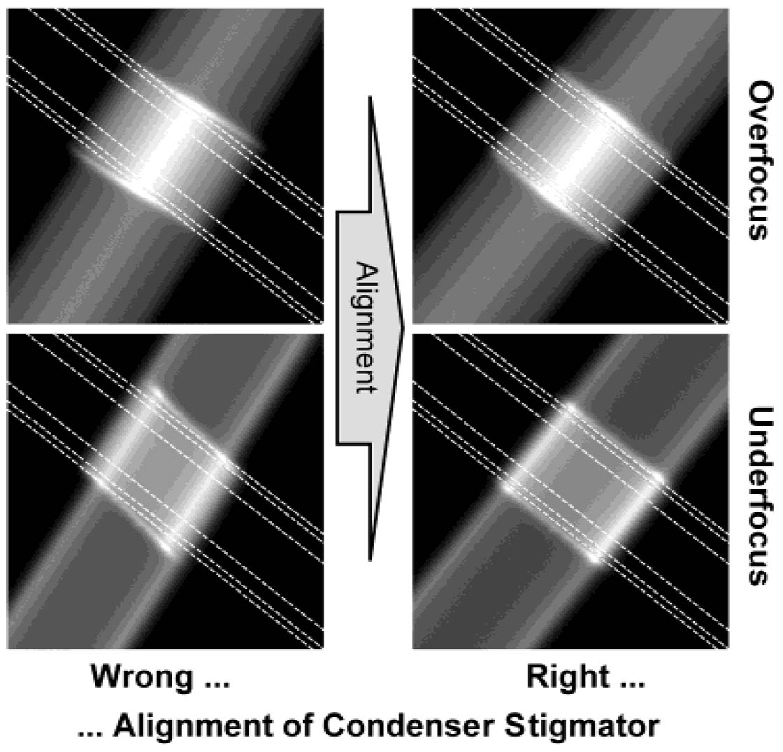
Figure 2603b. Alignment of the elliptical illumination perpendicular
to the biprism filament. [3]
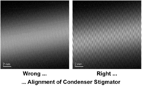
Figure 2603c. Gain of interference fringe contrast with illumination focusing.
[3]
k) Select a proper voltage at biprism filament.
l) Move the specimen into the interference region. Set the voltage at the filament at UF = 0 V, and make sure that the reference wave still pass through the empty and thus is not influenced by the specimen.
m) Set a proper defocus value:
In medium resolution applications for 2D-dopant profiling and imaging of magnetic stray fields, set the focus to Gabor defocus.
n) Set a proper exposure time by considering the noise level, and microscope and specimen stabilities. 10 – 15 seconds of exposure time is quite usual.
o) Take a hologram with the object in the TEM specimen.
p) Immediately after step o), move the object out of the field of view with goniometer (Don’t change any electron optical parameters).
q) Immediately after step p), take a reference hologram with exactly the same electron optical setup and exposure time.
r) Repeat steps o), p), and q) to take more images.
s) Repeat all steps from b) to q) if the experiment has taken very long time (considering the instabilities).
t) Select correct raw hologram images to analyze by looking at the interference fringe contrast and the sideband after Fourier transformation of the holograms.
u) Reconstruct the holograms with software on a personal computer (PC). For instance, this function can be found on the program Digital Micrograph (Gatan Company).
v) Correct the distortion-induced phase modulations:
v.1. Reconstruct the reference hologram using the same parameters as in m).
v.2.
Subtract the reconstructed reference phase from the reconstructed image phase, producing distortion-corrected image wave.
[1] Völkl, E., Allard, L.F. & Frost, B. (1995). A software package for the processing and reconstruction of electron holograms. J. Microsc. 180, 39–50.
[2] Harscher, A., Lenz, F. & Lichte, H. (1992). Electron holography
provides zero-loss images, 10th European Congress on Electron Microscopy, EUREM92, Granada, Last Minute Brochure,
35–36.
[3] Michael Lehmann, and Hannes Lichte, Tutorial on Off-Axis Electron Holography, Microsc. Microanal. 8, 447–466, 2002.
[4] Düker, H. (1955). Lichtstarke Interferenzen mit einem Biprisma
für Elektronenwellen. Zeitschrift für Naturforschung 10, 255–256.
[5] Allard, L.F. & Völkl, E. (1999). Optical characteristics of a
holography microscope. In Introduction to Electron Holography,
Völkl, E., Allard, L.F. & Joy, D.C. (Eds.), pp. 56–86. New York:
Kluwer Academics/Plenum Publishers.
|