
Chapter/Index: Introduction | A | B | C | D | E | F | G | H | I | J | K | L | M | N | O | P | Q | R | S | T | U | V | W | X | Y | Z | Appendix
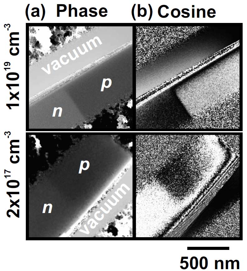
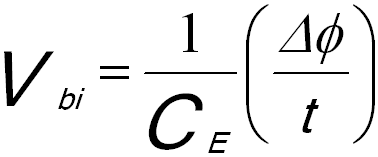
| Research and engineering applications of off-axis electron holography can be split into three main categories: Off-axis electron holography has been widely applied to characterize p-n junction specimens prepared using focused ion beam (FIB) technique. When there are no magnetic fields and diffraction contrast from the p-n junction, the change in phase of an electron as it passes through the specimen is given by, [2] Therefore, the phase of an electron is very sensitive to changes of dopant-induced potential in the specimens. In order to optimize the acquisition of holograms, in many cases, the microscopes need to be re-configured. For instance, Cooper et al. [2] turned off the probe corrector in their FEG FEI Titan microscope even though it had been installed. Both the objective lens and third condenser lens were turned off, and a Lorentz lens was used in order to extend the holographic field of view to 1500 x 700 nm2. Consequently, the fringe spacing in the holograms was 3.5 nm, resulting in a spatial resolution of ~10 nm in the reconstructed phase images. Figure 4305 shows examples of the phase images and cosine images of phases reconstructed from recorded holograms from p-n junctions at two different concentrations. The specimen thicknesses were ~400 nm determined by CBED. Two phenomena are very clear:
Figure 4305. (a) Phase images and (b) Cosine images of their phases for p-n junctions with the different dopant concentrations.
Adapted from [2]
From Equation 4305a, we can know that the built-in potential Vbi in the p-n junction can be measured by, [2] Note that for a FIB-prepared specimen, there is an electrically inactive layer on both surfaces so that t needs to be replaced by t-tinactive. Here tinactive is the total thickness of the inactive layers on both sides of the TEM specimen.
[1] W. D. Rau, P. Schwander, F. H. Baumann, W. Hoppner, and A. Ourmazd,
Phys. Rev. Lett. 82, 2614 (1999).
|
 ------------------------------ [4305b]