| The analytical electron microscopes (AEMs) especially have the advantage of performing analyses in a small area, typically <1 nm in diameter. In modern AEMs, this advantage is obtained by the flexibility of the illumination lens system that can provide a small-probe by changing the illumination condition from parallel to convergent.
STEM was invented by von Ardenne, German in 1937. [1] However, the application of STEM was not successful until several decades later, first performed by Albert Crewe in 1970.[2] Figure 4972a shows the positions of the detectors which can be installed in a STEM system. Depending on the scattering angle of the transmitted electrons, various signals can be detected as a function of the position of the scanning probe: BF (bright-field)-STEM, DF (dark-field)-STEM or HAADF (high angle annular dark field)-STEM. The DF detectors are annularly shaped to maximize the collection efficiency and the range of the collected scattering angles can be adjusted through the magnification of the intermediate lenses.
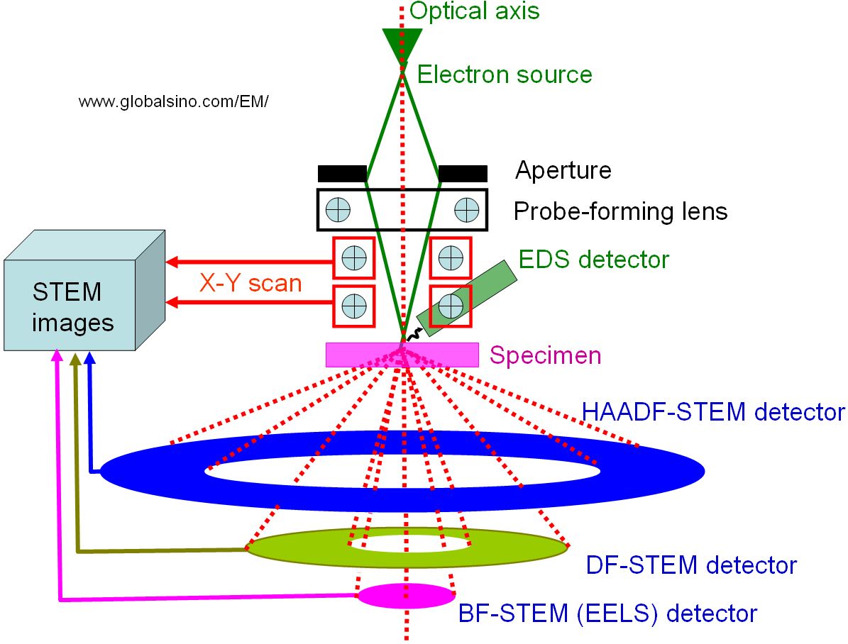
Figure 4972a. The positions of detectors in STEMs.
The schematics in Figure 4972b shows the electron optical column in a modern analytical electron microscope operated in STEM mode.
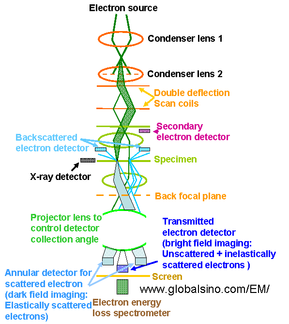
| Figure 4972b. Schematics of the electron optical column in a modern
analytical electron microscope operated in STEM mode. |
The performance of a STEM depends critically on the quality of the electron source that is determined by the source brightness.
Chemical analyses at high spatial resolutions are the domain of analytical
transmission electron microscopy (ATEM). These analyses are based on the collection of spectroscopic data originated from the inelastic interaction of the incident electron beam with the specimen. Therefore, these signals can be used to identify and quantify the concentrations of the elements and map their distributions, and even evaluate their chemical states at high spatial resolutions. There are mainly two techniques that are the core of AEM technique:
i) Owing to rapid instrumental developments during the past decade, electron energy-loss spectroscopy (EELS) offers now a spatial resolution close
to 0.1 nm and an energy resolution close to 0.1 eV. This development has been accompanied
by the introduction of numerous new techniques and methods for data
acquisition and analysis.
ii) EDS based on X-ray signals is normally a time-efficient technique.
Note that the use of a large convergence angle, as occurs in the STEM mode with a focused probe minimizes the problems of channeling enhanced X-ray emission and electron channeling in EELS measurements.
Except for the two techniques above, the other AEM techniques are:
iii) Convergent beam electron diffraction (CBED).
iv) Cathodoluminescence.
v) Auger electron spectroscopy (AES).
vi) Electron beam induced current (EBIC) imaging.
Though the later three techniques are also part of the AEM techniques available in the EMs but are less frequently added in commercial TEM or are used only as proof of concept.
To avoid specimen contamination, the specimen area requires a high vacuum level especially for chemical analysis in an analytical STEM when the electron beam is resting for a longer time in the small area. Ion pumps are often directly added to the specimen stage (especially for analytical EMs) or gun chambers of EMs to enhance the vacuum in these important regions.
In many cases, an optimal condition is needed for a particular analytical analysis and specific needs since:
i) It is not necessary that a specific technique is definitely the best choice for a certain element due to peak overlaps or no overlaps even though it is in general.
ii) Different sample thicknesses (for TEM and STEM) can affect the measurement differently.
iii) Different electron sources (field emission or thermionic sources) can affect the measurements differently.
Table 4972a. Summary of Analytical TEM/STEM Techniques.
Items |
Characteristics |
References |
Advantages of analytical TEM/STEM Techniques, compared to surface analysis techniques
|
Provides much better spatial resolution and the possible mapping |
|
Accelerating voltage of microscope |
Peak-to-background ratio (P/B ratio) in EELS spectra and EDS spectra increase with the accelerating voltages from 100 kV to 400 kV, resulting in an increase in the detection sensitivity of any trace elements |
|
EELS |
EELS |
Gives information on their local electronic structure
and bonding |
|
Low energy loss |
Band gap measurement |
page2406 |
| Determine the dielectric function across a HfO2/Si interface using Kramers–Kronig
analysis |
[5] |
| Obtain maps of effective mass by using cyclotron-resonance mass |
[4] |
TEM |
High-resolution TEM |
Investigates the atomic arrangement of individual
defects |
|
TEM + EELS |
High-resolution TEM + EELS |
Understanding of how the
atomic structure and physical properties are related |
|
Diffraction |
Strong diffraction in
a crystalline specimen |
Makes the interpretation of inelastic scattering more complicated, but
channeling directs the incident electrons down atomic columns and improves the spatial resolution of EELS |
[3] |
Holography |
Employs an interference phenomenon between the reference and diffracted waves to reconstruct an image of an object. Used for strain and activated dopant analysis |
page2612 |
Table 4972b. Summary of Capabilities of Analytical TEM/STEM Techniques.
Structure/information |
Techniques |
Characteristics |
Examples |
References |
Impurity induced strain |
HRTEM |
Higher spatial resolution |
As, B, P dopant in c-Si under limits of EDS and EELS detection |
page4312 |
Band gap |
Low energy EELS |
|
GaN, SiO2 |
page2406 |
Segregation at grain boundaries and interfaces
|
EELS |
Higher spatial resolution |
As in poly-Si |
page1271 |
| EDS |
Lower spatial resolution |
Ca in Mg-0.1Ca-0.2Zn alloy |
page1271 |
[1] Von Ardenne M, Beischer DZ. Electrochemie 1940;46:270–7.
[2] Crewe AV, Wall J, Langmore J. Science 1970;168:1338–40.
[3] Loane, R. F., Kirkland, E. J., and Silcox, J. (1988) Visibility of single heavy atoms on thin
crystalline silicon in simulated annular dark-field STEm images. Acta Crystallogr. A 44,
912–927.
[4]
Gass, M. H., Papworth, A. J., Beanland, R., Bullough, T. J., and Chalker, P. R., Mapping
the effective mass of electrons in III-V semiconductor quantum confined structures. Phys. Rev.
B 73, 035312 (6 pages), (2006).
[5] Park, J., and Yang, M., Determination of complex dielectric functions at HfO2/Si interface
by using STEM-VEELS. Micron 40, 365–369, (2009).
|
