Chapter/Index: Introduction | A | B | C | D | E | F | G | H | I | J | K | L | M | N | O | P | Q | R | S | T | U | V | W | X | Y | Z | Appendix
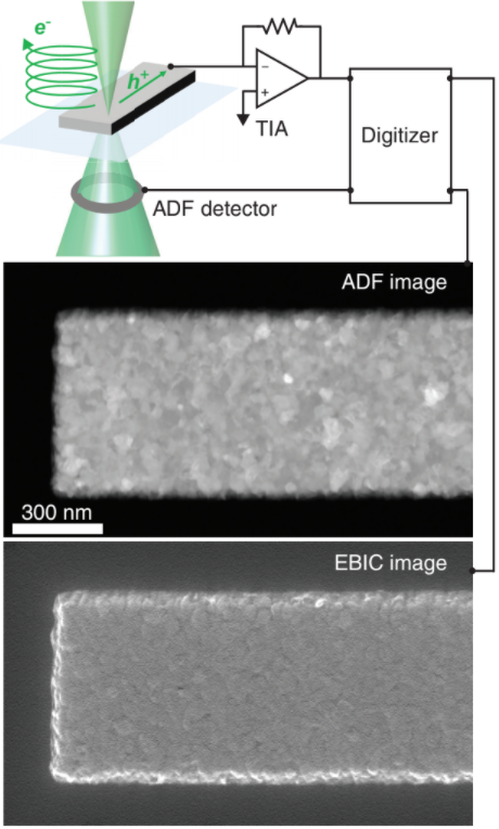
| Electron beam induced current (EBIC) was the first application of charging-induced effects in SEM and STEM. In this EBIC technique, a focused electron beam is scanned across a sample that is attached to a transimpedance amplifier (TIA) as shown in Figure 3831a. Then, associating the measured sample current with the beam position forms the EBIC image.
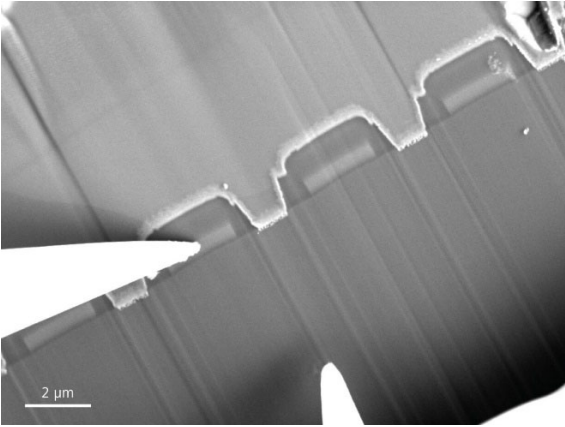
Because one primary electron can create thousands of electron-hole pairs, this generated current is formed by the separation of electron-hole pairs excited by a high energy e-beam (electron-beam) irradiating on semiconductor devices. For instance, the distinction at cross-sectional surfaces between n- and n+ regions was observed on a Si (silicon) wafer [1]. EBIC measurements demonstrated that shallow states exist at Σ3 coincidence site lattice (CSL) grain boundaries. [2] SEM image in Figure 3831b shows the nanoprobe placement for EBIC measurements of SiC MOSFETs.
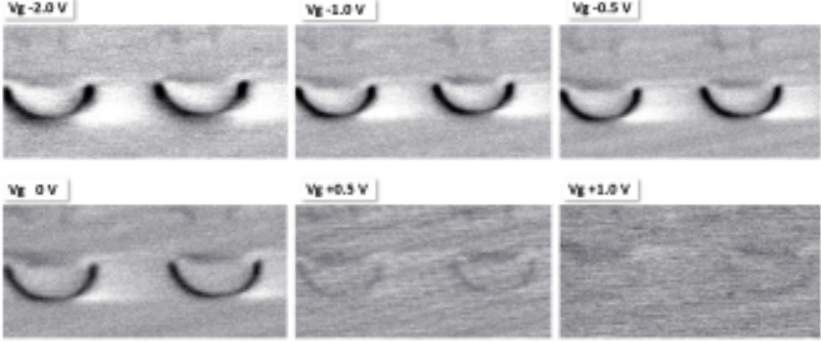
Figure 3831c presents EBIC images of the depletion zones between the P-body and N-drift region, shown as a function of gate voltage.
EBIC imaging has many applications of mapping:
[1] Kato, T., Matsukawa, T., Koyama, H., Fujikawa, K. and Shimizu, R.
(1975) Scanning electron microscopy of charging effect on silicon. J. Appl.
Phys., 46, 2288 - 2292.
|