Chapter/Index: Introduction | A | B | C | D | E | F | G | H | I | J | K | L | M | N | O | P | Q | R | S | T | U | V | W | X | Y | Z | Appendix
| Incident electrons suffer elastic and inelastic scattering. Electrons which exit a material surface must leave positive charges behind. Under steady-state EM imaging conditions, charging effects of substrate (in SEM) or film (in TEM) can take place. These effects mostly result from a dynamic competition between SEs (secondary electron) emission and trapping of some PEs (primary electrons) or generated SE. SE emission contributes to a positive charging, while PE/SE trapping contributes to a negative charging. For EM observations, a steady-state (or so-called equilibrium state) electrical balance can be established: I0 + Vs/Rs = It + I0η(t) + I0δ(Vs) -------------------------- [4465] where, Terms on the left-hand side of Equation 4465 represent current entering the irradiated volume from the incident beam (first term) and leakage current from the surrounding regions (second term). Terms on the right-hand side represent the loss of electrons by transmission (first term), by backscattering (second term), and by secondary emission (third term). The transmission term is zero for bulk SEM specimens, while it is non-zero for thin-film TEM, STEM, and SEM specimens. At high voltages of incident electrons (E0), the difference of ΔI (I0-It) is very small, meaning the electron absorption is negligible. Under a specific SEM imaging condition, the steady-state population of the charges is much smaller than estimated by the model of electron-hole pair generation, due to the escape, carrier diffusion, recombination and trapping of SEs (secondary electrons). As shown in Figure 4465, the higher incident voltage results in a larger amount of the implanted charge ΔQ comparing to the low incident voltage case. However, the charge density at the low incident voltage is larger than at the high incident voltage. For conductive materials in specimens, electric charges due to SEs are grounded immediately; therefore, the whole specimen area is neutralized. However, for insulating materials, e.g. organic materials and bio-materials, SEs accumulate and charge up, which causes damage and/or contamination on films. In EM measurement, especially in SEM measurement of a bulk material, when an electron beam hits a dielectric, its absorbed electrons accumulate on its surface due to the lack of a positive charge flowing from the ground.
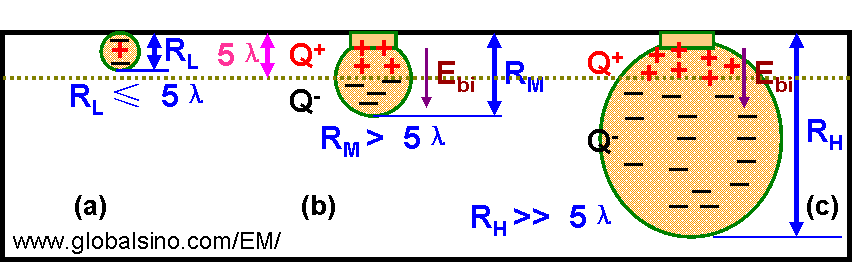
However, the actual charging process of an electrically isolated structure is very complicated and is determined by many factors: The resolution of electron microscopes (EMs) is partially limited by: The charging effect in TEM specimens can be reduced by lowering the electron beam intensity. For SEM, the charging effect is commonly reduced by specimen coating. However, one needs to be aware that the specimen coating can induce spurious X-rays if he is doing EDS measurements. Sample Thickness Effect on Sample Charging: Based on the dependence of interaction volume and maximum escape depth on PE (primary electron) beam energy, there are three different cases regarding SE emissions: i) RL ≤ 5λ, ii) RM > 5λ, and iii) RH >> 5λ as shown in Figure 4465 (R is maximum interaction volume and λ is maximum escape depth). For the case of R ≤ 5λ, the two positive and negative charge areas are very close. For the cases of R > 5λ and R >> 5λ, there are two distinct regions inside the interaction volume: a thin near-surface layer with thickness T ~ 5λ in positive charge Q+, and a negatively charged bulk (Q-) with a thickness of about (R–T). As a result, the implanted charge is ΔQ = Q+ + Q-, and the built-in electric field (Ebi) governed by ΔQ is established.
[1] R.F. Egerton, P. Li, and M. Malac, Radiation damage in the TEM and SEM, Micron 35 (2004) 399–409.
|