Chapter/Index: Introduction | A | B | C | D | E | F | G | H | I | J | K | L | M | N | O | P | Q | R | S | T | U | V | W | X | Y | Z | Appendix
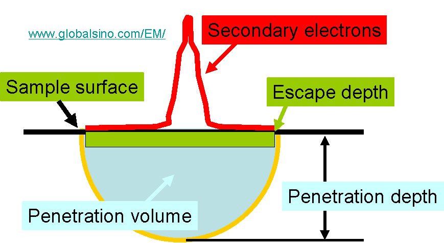
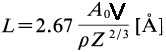
| Because of the low energies of secondary electrons (SEs), SEs generated more than a certain distance (maximum escape depth, L) below the surface cannot escape from the specimen. SEs that do escape are produced within a distance of 2 - 5 nm of the surface in most materials.. More accurately speaking, previous research has shown that the mean escape depth is 1 – 5 nm for metals and 10 – 20 nm for insulators, respectively. [1] Ono and Kanaya simplified the escape depth calculation by correlating it with periodic properties of the elements, given by: [2] A0 -- The atomic weight in a.m.u. For doped materials, the net escape depth can also be evaluated based on Equation [4799a]. Assuming A elements are dopants and B elements are host atoms; thus, L in the materials can be estimated by, Based on Equation [4799a] we can obtained the escape depths of graphite (Lc) and of hydrogen solid (LH) are 4.81 nm and 19.18 nm, respecitively. For the hydrogen-implanted graphite, assuming H/C ratio is equal to 1, then we can know L is equal to 3.85 nm by following the Equation [4799b]. The smaller L in the hydrogen implanted graphite than that in pure graphite is due to the increase in atomic electrons interacting with SEs in the implanted material. Figure 4799a shows the schematic of penetration depth and volume in comparison with escape depth.
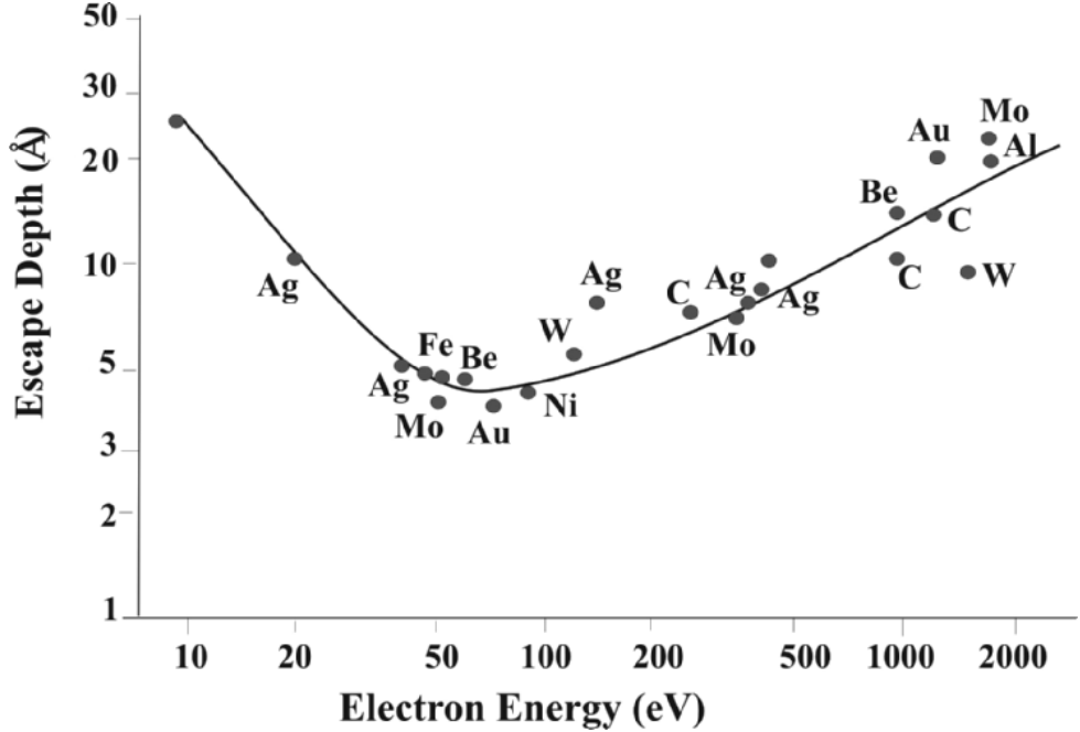
Figure 4799a. The schematic of penetration depth and volume in comparison with escape depth. The maximum escape depth T of the SE is independent of the PE (primary electron) beam energy and does not exceed T ~ 5λ [3] ((λ stands for mean free Figure 4799b shows that the probability of escape from the sample surface without inelastic scattering is dependent on the energy of the electrons. For kinetic energy ~50–100 eV (i.e., minimum λ of ~5–10 Å), the surface sensitivity is maximum.
[1] H. Seiler, Z. Angew. Phys. 22 (1967) 249.
|
 ----------------------------------------------- [4799a]
  ---------------------------------------- [4799b]