Chapter/Index: Introduction | A | B | C | D | E | F | G | H | I | J | K | L | M | N | O | P | Q | R | S | T | U | V | W | X | Y | Z | Appendix
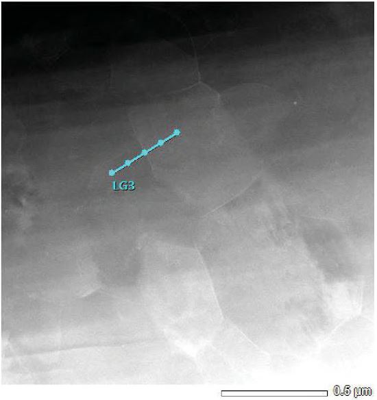
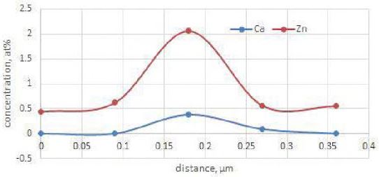
| Figure 1271a (a) shows a scanning transmission electron microscopy (STEM) high angle annular dark field (HAADF) image taken from an extruded Mg-0.1Ca-0.2Zn alloy. Such STEM image presents Z-contrast from composition but eliminates diffraction contrast. In this image, the grain boundaries at higher contrast are observed clearly, indicating high concentrations of elements with a high atomic number(s). The grain size is about 500 nm and the grain boundaries are not only straight and sharp in the image plane but also sharp and longer than the thickness of the TEM specimen along the electron beam. Therefore, EDS line scan could be employed to study elemental depletion and segregation at the grain boundaries. Figure 1271a (b) shows such a line scan, presenting a maxima in the concentrations of Ca and Zn occured at the grain boundary.
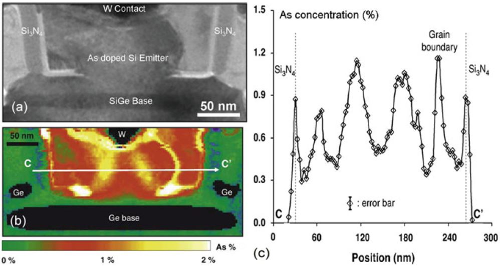
Figure 1271b shows an As-L2,3 EELS map and a line scan of As-doped Si BiCMOS n-p-n transistors with As detection sensitivity of 1019 cm–3 at a spatial resolution of ~2 nm, measured in a STEM system with an incident beam energy of 120 keV.
[1] Alok Singh, Kiran Solanki, Michele Manuel, Neale Neelameggham, Magnesium Technology, 2016.
|