=================================================================================
Figure 3557a schematically shows the relationship between the 7 crystal systems, 14 Bravais Lattices, 32 point groups, and 230 space groups.
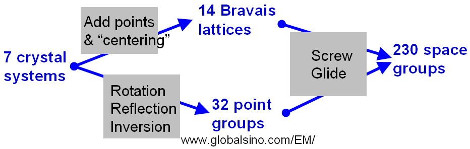
Figure 3557a. The relationship between the 7 crystal systems,
14 Bravais Lattices, 32 point groups, and 230 space groups.
The operation of a glide plane is a reflection and a translation of half a lattice spacing parallel to the plane (namely, glide plane = reflection + translation). In other words, a glide plane is a mirror followed by a translation of 1/2 the length of the vector in the plane of the mirror as shown in Figure 3557b.
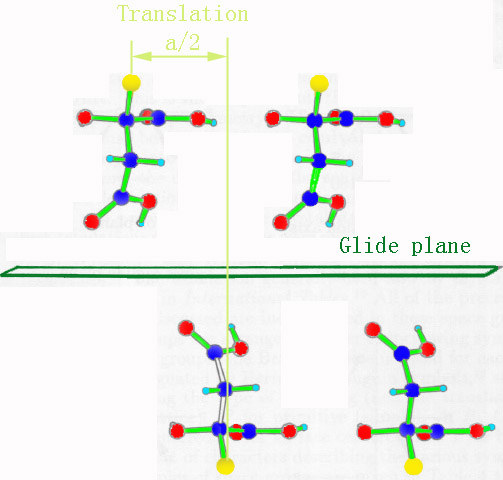
Figure 3557b. Glide planes: A combination of mirroring with a/2 translation. Here, a is the lattice constant.
As shown in Table 3557a, the translation can be along an axis in the plane (a,b, and c) or along the diagonal (n and d).
Table 3557a. Nomenclature for glide planes.
Designation |
Glide direction |
Glide magnitude |
Remarks |
a-glide, b-glide, or c-glide |
<100> |
1/2 axis length axis length |
|
n-glide |
<110> |
1/2 face diagonal |
Glide translation along with half a face diagonal |
d-glide |
<110> |
1/4 face diagonal |
Glide along a quarter of either a face or space diagonal of the unit cell and is often called the diamond glide plane as it features in the diamond structure |
e-glide |
|
|
Two glides with the same glide plane and translation along two (different) half-lattice vectors |
Table 3557b lists the dominating slip planes and slip directions for common crystal structures.
Table 3557b. Dominating slip planes, slip directions and stable Burgers vector for common crystal structures.
Crystal structure |
Dominating slip planes and others |
Slip direction |
Stable Burgers vector |
Note |
Material examples |
|
{111}: 4 octahedral planes (111), (1-11), (11-1), and (-111) |
<110>: 6 <110> directions in each octahedral plane |
a/2 <110> |
Each of the directions is common to two octahedral planes, and thus there are 12 slip systems in total. |
Cu, Ag, Au, Al, Ni, brass, some stainless steels |
Possible plane: (100) |
<10-1> |
|
Mono-atomic BCC metals
|
{110}: 12 possible planes |
<111>: 4 slip directions [1-11], [-111], [-11-1] and [1-11] for each plane |
a/2 <111> |
48 possible combinations of slip plane and slip direction in total |
Li, Na, K, Fe, V, Cr, Mn, Cb, Mo, W, Ta, most steels |
| {112}: 24 possible {112} planes |
<111>: 2 slip directions [-1-11] and [11-1] for each plane |
a/2 <111> |
48 possible combinations of slip plane and slip direction in total |
| {123}: 48 possible planes |
<111>: 2 possible slip directions [-1-11] and [11-1] for each plane |
<100> |
96 possible combinations of slip plane and slip direction in total |
| Mono-atomic SC |
|
|
<100> |
|
|
|
{001} (or {0 0 0 1}) |
<110> |
a/2 <110> (or 1/2<1 1 -2 0>) |
|
Be, Mg, Zn, Sn, Ti, Co, graphite, metals and alloys |
| {101} |
<110> |
a/2 <110> (or 1/2<1 1 -2 0>) |
| {112} |
<113> |
a + c |
| {2 1 0} (or {10-10}) |
|
<0 0 1> (or <0 0 0 1>) |
|
{111} |
<110> |
a/2 <110> |
|
Diamond, Si, Ge |
|
|
|
<100> |
|
|
|
{110} |
<110> |
a/2 <110> |
|
NaCl, LiF, MgO, AgCl |
| Sometimes {100} |
|
|
|
|
Gjönnes-Moodie extinction [1] is a type of dynamical extinctions in some electron diffraction patterns. This extinction may occur, for instance, in the presence of a screw-axis or a glide planes because the multiple scattering contributions cancel each other even in the dynamical scattering regime due to destructive interference between contributions with opposite phase.
A glide dislocation is generally a line boundary between the slipped and unslipped portions of the glide (slip) plane. The line is not necessary to be straight. When it is curved some parts can be a screw dislocation and some parts an edge dislocation. For a given sense vector that points in one direction along the dislocation, the Burgers vector is invariant.
With stereographic projections, we can easily visualize crystallographic features:
i) Crystal symmetry.
ii) Slip planes and directions.
iii) Crystal planes and orientation relationships.
iv) Grain orientations.
Table 3557c. Reflection conditions due to the existence of glide planes.
| Glide plane |
Reflection condition |
Reflections involved |
Zonal extinction law |
| Along a |
h = 2n |
|
0 k l for k + l = 2n + 1 (k + l = odd) |
| Along b |
k = 2n |
0kl for plane ⊥ a |
|
| Along c |
l = 2n |
h0l for plane ⊥ b |
h k 0 for h + k = 2n + 1 (h + k = odd) |
| Along n |
h + k; k + l or h + l = 2n |
hk0 for plane ⊥ c |
|
| Along d |
h + k; k + l or h + l = 4n |
|
|
The electron diffraction pattern in Figure 3557c shows both ZOLZ and FOLZ reflections obtained from Zr41Ti14Cu12.5Ni10Be22.5 in [100] zone axis. Due to the absence of ZOLZ/FOLZ periodicity difference, we can know that there is no glide plane perpendicular to the [100] direction.
![Electron diffraction pattern obtained from Zr41Ti14Cu12.5Ni10Be22.5 in [100] zone axis](image2/3902c.gif)
Figure 3557c. Electron diffraction pattern obtained from Zr41Ti14Cu12.5Ni10Be22.5 in [100] zone axis. The lattice parameters are a = 0.34 nm, and c = 1.137 nm.
[2]
A vertical glide plane results in a mirror line in the CBED pattern. At Bragg condition, a horizontal twofold axis or twofold screw axis in the ZOLZ along g presents a mirror line of symmetry onto disk g, and this line runs normal to g, and a horizontal mirror plane or glide plane leads to a centric distribution of intensity in every CBED disk. The odd order reflections in the direction of the axis will be forbidden if the glide plane is parallel to the electron beam. For a screw axis or glide plane, if the projection of the unit cell in the beam direction has a symmetry, then the forbidden reflections would not be fully forbidden but would obviously be very weak.
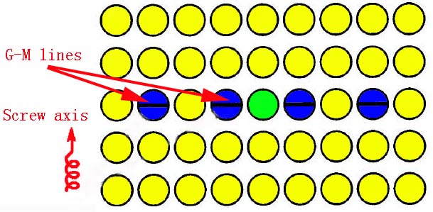
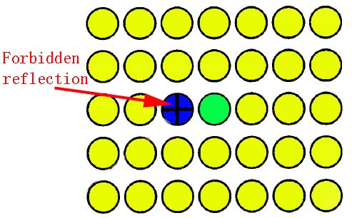
In Figure 3557d, the dark bands indicate that the electron beam is either parallel to a glide plane or vertical to a screw axis in the crystal, and the black crosses refer to forbidden reflections.
Figure 3557d. Schematic illustration of G-M lines: (a) A screw axis perpendicular to the electron beam; and (b) Black crosses indicating forbidden reflections. The green disc denotes the transmission beam, the blue discs denote forbidden reflections, and the yellow discs denote the diffraction beams.
For instance, the forbidden reflections in crystals with P21/c (14) space group are caused by 21-screw axis and n-glide plane.
[1] Gjönnes, J., Moodie, A.F., 1965. Extinction conditions in the dynamical
theory of electron diffraction. Acta crystographica 19, 65–67.
[2] Q. Wei, N. Wanderka, P. Schubert-Bischoff, and M-P. Macht, S. Friedrich, Crystallization phases of the Zr41Ti14Cu12.5Ni10Be22.5 alloy after slow solidification, J. Mater. Res., 15 (8) 1729, (2000).
|