Chapter/Index: Introduction | A | B | C | D | E | F | G | H | I | J | K | L | M | N | O | P | Q | R | S | T | U | V | W | X | Y | Z | Appendix
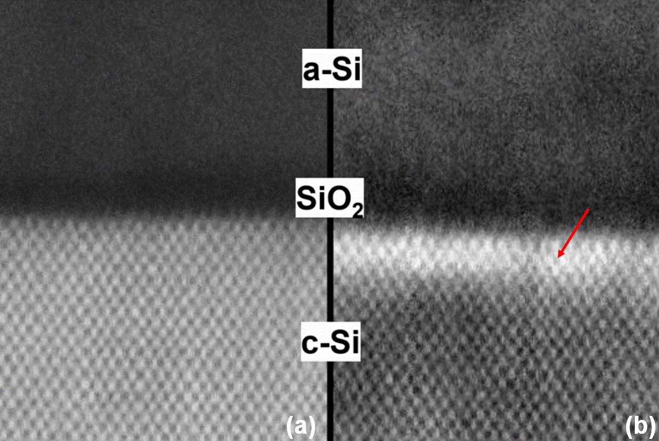
| Table 1194a lists the possible contrast mechanisms of bright-band in the Si (silicon) crystal at an a-SiO2/c-Si interface or an a-Si/c-Si interface in an ADF-STEM image. Table 1194a. Possible contrast mechanisms of bright-band of c-Si at a-Si or a-SiO2/c-Si interfaces.
Other factors such as sample thickness effect in zone-axis crystals [7] and detector inner angle, as shown in Table 1194b, may also affect the appearance of strain contrast in ADF images. In the existing of strain fields, the scattering of electrons results in different angular distributions and thus the intensity collected by the ADF detector from the strained region can be different than that from the strain-free region, resulting in strain contrast. The thickness dependence of strain contrast originates from the propagation process of the electron beam with the channeling effect [8-10, 1] inside a zone-axis crystal, while such channeling effect is not significant in very thin (<10 nm) TEM samples.
As shown in Figure 1194a, when the strain amplitude increases, the channeling effect decreases, which is also called dechanneling. Therefore, the strain fields cause dechanneling.
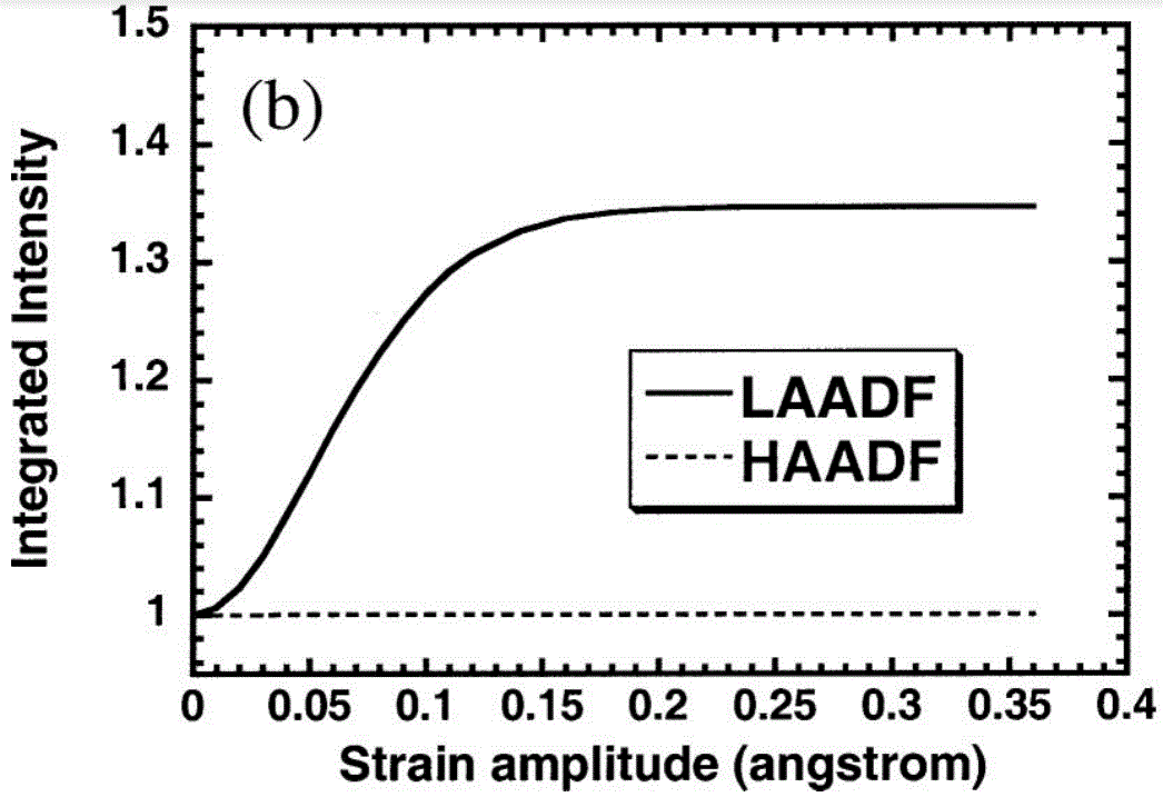
Figure 1194b shows the integrated ADF-STEM intensities versus strain amplitude of crystalline silicon (Si) over LAADF and the HAADF detectors. The LAADF signal increases when a strain field is introduced in LAADF image for thick TEM samples, while the HAADF signal stays essentially constant as strain amplitude increases.
Note that, as shown above, the dechanneling contrast in LAADF images is induced by strain field in crystals, which originates from impurities, interface effect, mechanical bending, etc.
[1] R. R. Vanfleet, M. Robertson, M. McKay, and J. Silcox, Characterization and Metrology for ULSI Technology (American Institute of Physics, New York, 1998), p. 901.
|