| Table 1195a lists the possible contrast mechanisms of bright-band in the Si (silicon) crystal at an a-SiO2/c-Si interface or an a-Si/c-Si interface in an ADF-STEM image.
Table 1195a. Possible contrast mechanisms of bright-band of c-Si at a-Si or a-SiO2/c-Si interfaces.
Possible contrast mechanism of bright-band in c-Si |
a-SiO2/c-Si interface |
a-Si/c-Si interface |
| Roughness of the interface |
Yes [2] |
No [5] |
| Associated
with oxygen segregation |
Yes [3] |
-- |
| Dopant with annealing temperature |
|
Yes [6] |
| With a strain field |
Yes [4] |
Yes [5] |
Other factors such as sample thickness effect in zone-axis crystals [7] and detector inner angle, as shown in Table 1195b, may also affect
the appearance of strain contrast in ADF images. In the existing of strain fields, the scattering of electrons results in
different angular distributions and thus the intensity collected by the ADF detector from the strained region can be different than that from the strain-free region, resulting in strain contrast. The thickness dependence of strain contrast originates from the propagation process of the electron beam with the channeling effect [8-10, 1] inside a zone-axis crystal.
| Table 1195b. Strain fields in crystalline silicon layers at a-Si/c-Si interface. [5]
If the ADF intensity from the strained
region is higher than that from the strain free region, this contrast is then
defined as a positive contrast and negative contrast if the
strained region appears darker than the strain-free region. |
ADF |
TEM sample thickness |
Strain contrast |
| LAADF |
<10 nm |
Negative |
| >15 nm |
Positive |
| HAADF |
<10 nm |
Negative |
| >15 nm |
Negative |
As shown in Figure 1195, when the strain amplitude increases, the channeling effect decreases, which is also called dechanneling. Therefore, the strain fields cause dechanneling.
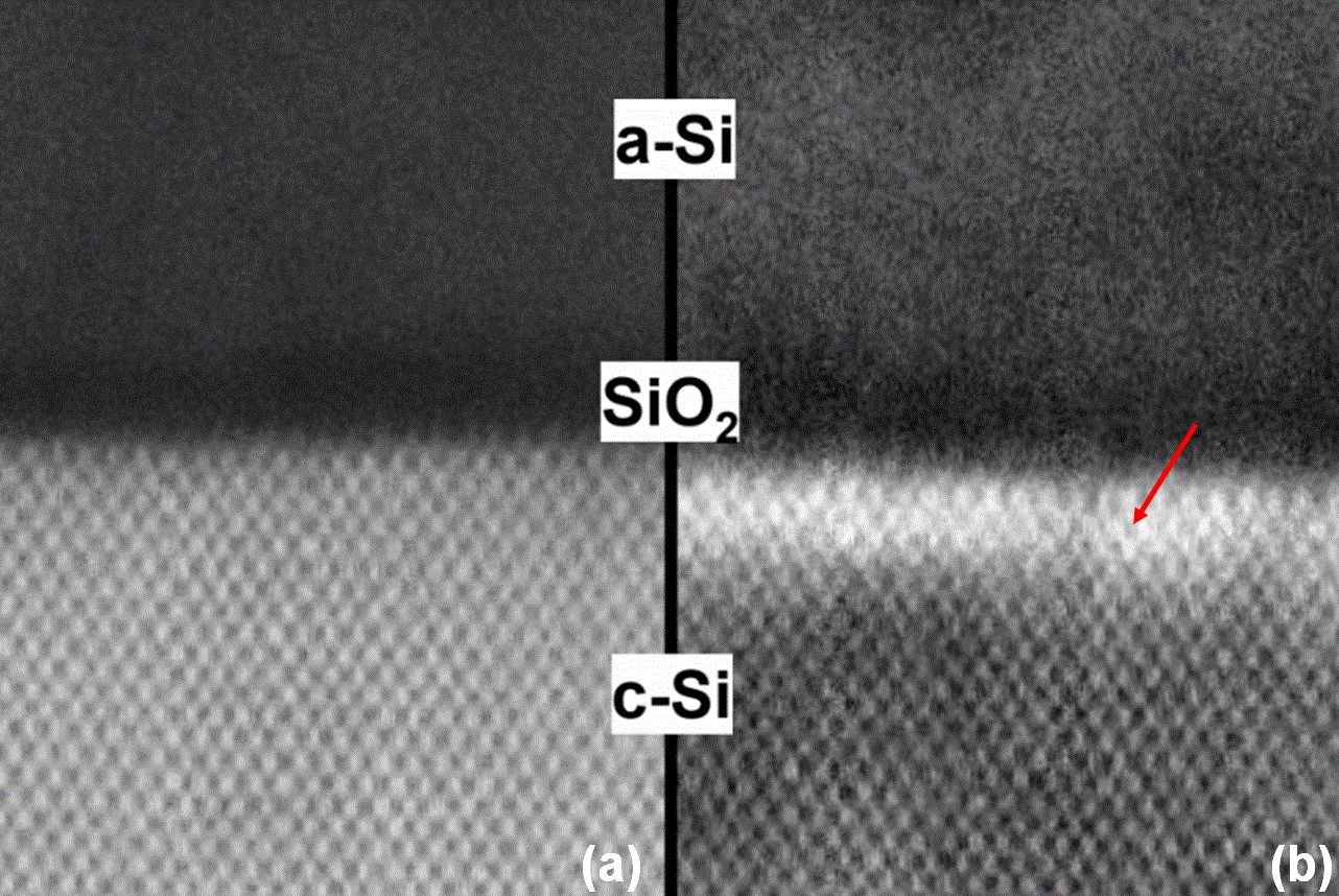
| Figure 1195. (a) HAADF image along (110) zone axis of silicon (Si), (b) LAADF images. The strained region is marked by the red arrow. Adapted from [5] |
[1] R. R. Vanfleet, M. Robertson, M. McKay, and J. Silcox, Characterization and Metrology for ULSI Technology (American Institute of Physics, New York, 1998), p. 901.
[2] D. A. Muller, T. Sorsch, S. Moccio, F. H. Baumann, K. Evans-Lutterodt, and G. Timp, Nature, (London) 399, 758 (1999).
[3] P. E. Batson, IBM J. Res. Dev. 44, 477 (2000).
[4] G. Duscher, S. J. Pennycook, N. D. Browning, R. Rupangudi, C. Takoudis, H.-J. Gao, and R. Singh, Characterization and Metrology for ULSI Technology (American Institute of Physics, New York, 1998), p. 191.
[5] Zhiheng Yu, David A. Muller, and John Silcox, Study of strain fields at a-Si/c-Si interface, J. Appl. Phys. 95, 3362 (2004).
[6] S. Hillyard and J. Silcox, Ultramicroscopy 58, 6 (1995).
[7] S. Hillyard and J. Silcox, Ultramicroscopy 52, 325 (1993).
[8] D. Hugo, H. Kohl, and H. Rose, Ultramicroscopy 17, 303 (1985).
[9] R. F. Loane, E. J. Kirkland, and J. Silcox, Acta Crystallogr., Sect. A: Found. Crystallogr. 44, 912 (1988).
[10] S. Hillyard, R. F. Loane, and J. Silcox, Ultramicroscopy 49, 14 (1993).
|
