Chapter/Index: Introduction | A | B | C | D | E | F | G | H | I | J | K | L | M | N | O | P | Q | R | S | T | U | V | W | X | Y | Z | Appendix
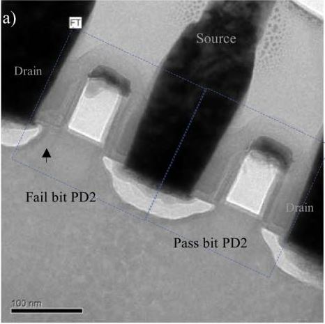
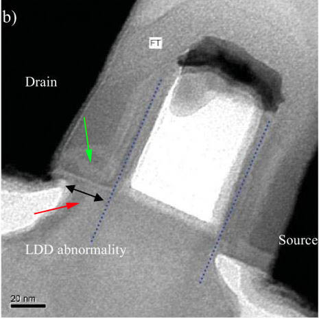
| The TEM images in Figure 1209 show that the light doped drain (LDD) on the drain side of the fault pull down transistor (PD2) is partially blocked by a space particle. Note that the TEM sample was stained in a mixture solution of HNO3, HF and CH3COOH before TEM observation.
[1] Jie Su, Sanan Liang, Yoyo Wen, May Yang, Linfeng Wu, Chorng Niou, Xianfeng Chen, and Gary Zhao, Electrical Signature Verification of a Lightly Doped Drain Profile Abnormality in a 65 nm Device via Nano-Probing and Junction Stain TEM, ISTFA 2009: Conference Proceedings from the 35th International Symposium for Testing and Failure Analysis, November 14-19, 2009, San Jose, USA.
|