Chapter/Index: Introduction | A | B | C | D | E | F | G | H | I | J | K | L | M | N | O | P | Q | R | S | T | U | V | W | X | Y | Z | Appendix
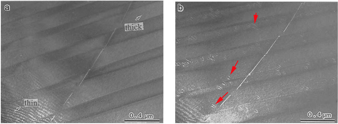
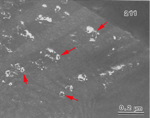
| With the conventinal TEM specimen preparation method, interstitials and vacancies can be generated by Ar ion milling at TEM surfaces. However, the diffusivity of the interstitials is normally larger than that of the vacancies and thus, the diffusion of interstiital ions is easily induced in specimen preservation and/or in TEM observations at room tempratrue, resulting in development of dislocation loops, sometime associated with stacking faults. For instance, Figure 1286a shows TEM images observed in a superconductive YBa2Cu3O7-y (YBCO) crystal just after ion-milling and after subsequent preservation in a silica-gel desiccator for two weeks. Dislocation loops in Figure 1286a (b) were observed clearly, created during the specimen preservation and their density did not vary with increase in specimen thickness. The same kind of dislocation loops also were occasionally formed due to electron irradication on ion-milled specimens during TEM observation as shown in Figure 1286b. Note that the loops were generated in the specimens prepared by Ar ion milling at both room temperature and 77 K but not in the ones prepared by crushing or chemical etching. Therefore, the researchers [1] proposed that the point defects, including interstitials and vacancies, were initiated by irradication of Ar ions and the dislocation loops grew by electron-induced diffusion and/or subsequent specimen preservation. However, both TEM specimen preparation methods of crushing and chemical etching do not obviously generate interstitials and vacancies.
[1] Yoshitomo Tanaka, Yoshitsugu Tomokiyo, Yasuhiro Omori and Yoko Suyama, Dislocation loops in melt-textured YBa2Cu3O7-y, Advances in Superconductivity VI, edited by Toshizo Fujita, Yuh Shiohara.
|