
Chapter/Index: Introduction | A | B | C | D | E | F | G | H | I | J | K | L | M | N | O | P | Q | R | S | T | U | V | W | X | Y | Z | Appendix
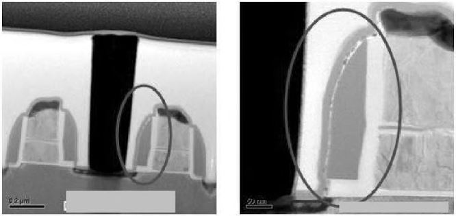
| Cobalt silicide stringer, causing gate to drain leakage, had been observed in MOS structures as shown in Figure 1292a.
Figure 1292a. Cobalt silicide stringer causing gate to drain leakage [1]. Abnormal CoSix spikes under cobalt silicide film were also found in IC devices (e.g. Figure 1292b). Such spikes and Si/silicide interface roughness and thus various defects can cause unacceptable high junction leakage (junction shorting) because the spikes encroach on the junction edge when the silicide thickness becomes larger [3, 4]. In this case, the consumed silicon depth gets too large so that the silicide-silicon interface gets too close to the p-n junction. Goto et al. proposed that the leakage was driven by an area effect as opposed to perimeter effects [5, 6]. They stated that the leakage occurred at the phase transition temperature from Co2Si to CoSi as a results of CoSi spikes through the metallurgical junction. The stress-induced Co2Si/CoSi/Si triple points, leading to area spiking, result in significant junction leakage in ultra-shallow junctions. In fact, this leakage is caused by junction depletion region encroachment upon the silicide-silicon interface. On such failing samples, it was observed by AFM measurements that the surfaces of p+ diffusion areas were smoother than the n+ diffusion areas after the cobalt silicides had been removed with dilute HF [3].
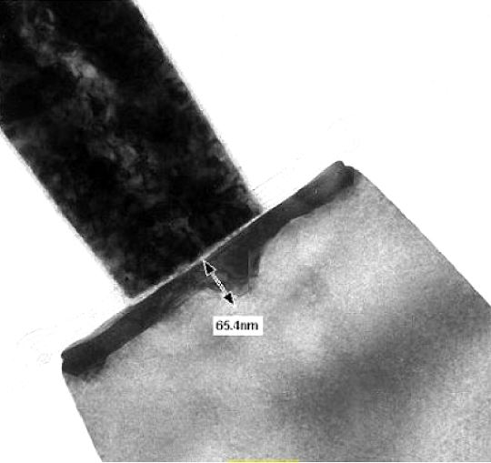
Figure 1292b. Abnormal cobalt silicide spike [2]. Note that, for ultra-shallow contact areas, it is critical to form smooth, conformal cobalt disilicide (CoSi2) without facets or voids for microelectronic device reliability. [8] On the other hand, to maintain the junction leakage within the tolerable range, the silicon consumption depth is limited to half of the source/drain contact junction depth. [7] Figure 1292c presents a Z-contrast STEM image of a failing transistor. The image highlights a defect, specifically a cobalt silicide protrusion under the gate. The bright areas in the image represent the cobalt silicide, which has a higher atomic weight compared to the surrounding silicon substrate and oxide layers. The elemental composition of the protrusion was confirmed through STEM-EDS spectral mapping (as shown in the inset of the figure), which detected cobalt in the region. This silicide protrusion can lead to electrical shorts and affect device performance .
[1] ISTFA 2009: Conference Proceedings from the 35th International Symposium for Testing and Failure Analysis.
|
![Z-contrast STEM image of the failing transistor [29]. The bright area protruding under the gate indicates the presence of a heavier element, and the STEM-EDS spectral map (inset) of the cobalt signal from the boxed region confirms that the protrusion is cobalt silicide](image2/1292a.png)