Chapter/Index: Introduction | A |
B |
C |
D |
E |
F |
G |
H |
I |
J |
K |
L |
M |
N |
O |
P |
Q |
R |
S |
T |
U |
V |
W |
X |
Y |
Z |
Appendix
Point Defects Created in FIB-EM Sample Preparation
| As shown in Figiure 1311, in FIB-EM sample preparation, point defects (e.g. vacancies and interstitials) are created underneath the amorphized layer. These point defects can:
i) Modulate electronic structure of the material and affect TEM holography and SCM (scanning capacitance microscopy) signal;
ii) Lead to formation of dislocation loops;
iii) Affect diffraction contrast TEM.
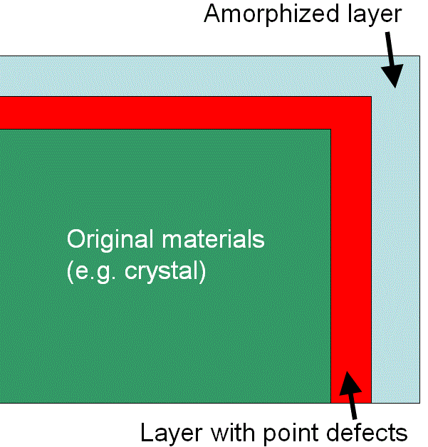
| Figiure 1311. Defects (point defects and amorphous layer) created in FIB-EM sample preparation. |
|
