Chapter/Index: Introduction | A | B | C | D | E | F | G | H | I | J | K | L | M | N | O | P | Q | R | S | T | U | V | W | X | Y | Z | Appendix
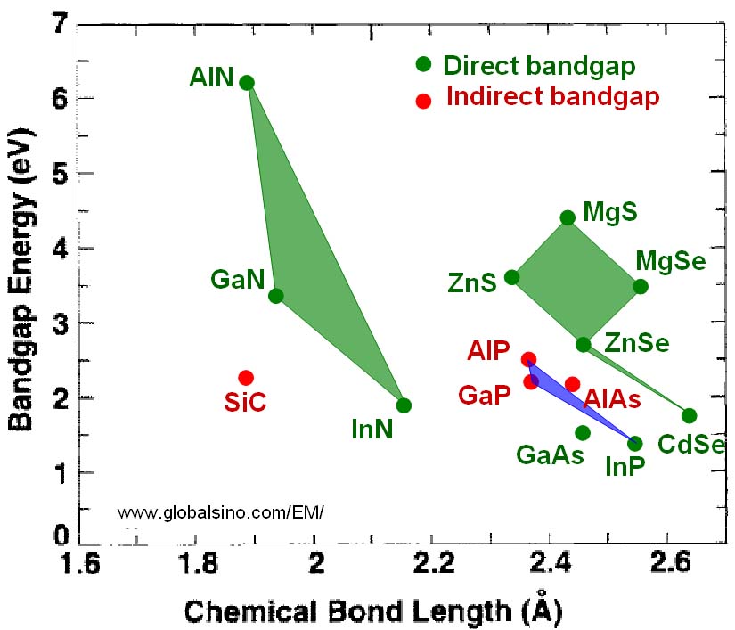
| GaN has recently developed into an important semiconductor for optical and electronic applications. For instance, GaN crystals and thin-films are used to form highly efficient light emitting diodes (LEDs) in the short wavelength region of the visible spectrum [2] and the ultraviolet (UV), and blue-emitting laser diodes [3]. The GaN based thin films, for instance, can be grown by metalorganic chemical vapor deposition (MOCVD) on (0001) sapphire substrates. The dislocation densities in these films are in the order of 1010 cm-3, propagating in the growth direction and cross the active region of the devices.[4] Note that one fabrication issue of this application is that high reflectivity mirror facets are hard to obtain because of the large misalignment between the sapphire substrate and GaN-based materials [6]. Figure 2093a shows bandgap and chemical bond length for semiconductors used in visible LEDs (light emitting devices).
Figure 2093a. Bandgap and chemical bond length for semiconductors used in visible LEDs (light emitting devices). Adapted from [1] Table 2093a shows the lattice properties of GaN. It is difficult to grow GaN bulk crystals due to the high melting temperatures and high equilibrium vapor pressures at their melting temperatures. Table 2093a. The lattice properties of GaN.
Due to a large lattice mismatch with the substrates, the material possesses an overall high density of threading dislocations. Table 2093b shows the lattice mismatch (%) between the substrates and epitaxial layers, and the resulting misfit dislocation separation (in Å) corresponding to complete misfit relaxation for the basal plane interfaces. Table 2093b. The lattice mismatch (%) between the substrate and epitaxial layers, and the resulting misfit dislocation separation (in Å).
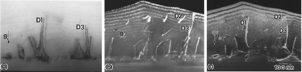
Note that GaN has poor native oxides. Figure 2093b shows three two-beam TEM images taken from the same area of a GaN thin film grown by MOCVD on N-face of a GaN bulk single crystal substrate [5]. The images present three types (D1, D2, and D3) of dislocations. The conventional diffraction contrast analysis suggested that the dislocations have the Burgers vectors listed in Table 2093c.
Figure 2093b. TEM images taken from the cross-section of a GaN homoepitaxial film showing a variety of dislocations: (a) Bright field with g1 = [0002]; (b) Dark-field image with g4 = [01-10]; and (c) Dark-field image with g5 = [1-102]. Adapted from [5] Table 2093c. Standard g·b analysis obtained by observing the dislocation image strength in dark-field and bright-field images in Figure 2093b. Based on the invisibility criterion, a specific dislocation may or may not display in a image. For instance, the two-beam bright-field TEM image in Figure 2093b (a) can not show D2 because g1·b = 0 as indicated in Table 2093c.
Table 2093d. Magnitudes of Burgers vectors of dislocations in nitride semiconductors (in Å).
Three different types of screw dislocations can present in GaN: open core, filled core, and full core screw dislocations.
[1] Ponce, F. A. and Bour, D.P., Nature, 386, (1997) 351.
|
|||||||||||||||||||||||||||||||||||||||||||||||||||||||||||||||||||||||||||||||||||||||||||||||||||||||||||||||||||||||||||||||||||||||||||||||||||||||||||||||