Chapter/Index: Introduction | A | B | C | D | E | F | G | H | I | J | K | L | M | N | O | P | Q | R | S | T | U | V | W | X | Y | Z | Appendix
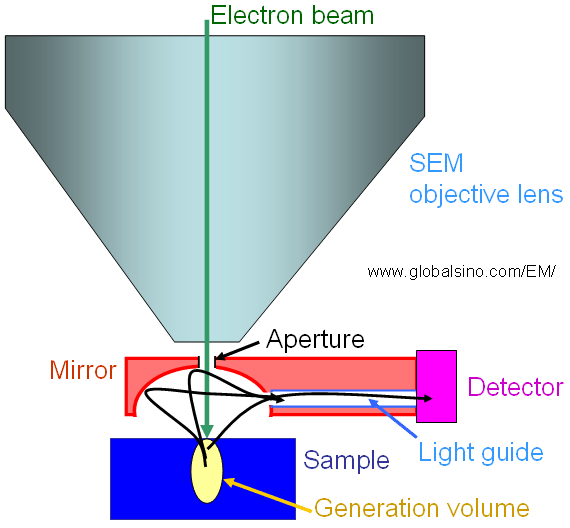
| Cathodoluminescence (CL) technique in SEM is widely used for examining optical properties of electronic structures. In this technique, the sample is excited by the electron beam so that the beam generates electron-hole (e-h) pairs which diffuse and recombine randomly. In the CL technique, the electrons in a semiconducting material, e.g. in III-V devices, are promoted from the conduction band to the valence band due to the excitation of the high energy incident-electrons in the SEM. The emitted CL photons result from the recombination of these excited electrons; therefore, the detected CL photons provide information on local bandgap variations that may originate from strain, defects, impurities, alloy fluctuations, etc. Figure 2421 shows the schematic illustration of cathodoluminescence setup. In the SEM system, the electron beam from the electron gun passes through an aperture in the paraboloidal mirror towards the sample surface. The generated photons are collected by the mirror and then sent through a light guide to the photon's detector (CCD camera or photomultiplier). The CL signal represents the local properties of the specimen.
Figure 2421. Schematic illustration of cathodoluminescence setup.
Recently, high spatial resolution CL as an optical spectroscopy technique in electron microscope has widely been used in non-destructive failure analysis and defect inspection of electronic devices. The correlation of surface morphology in SEM contrast in combination with spectrally resolved and highly sensitive of material composition from the CL emission, provides a pathway in non-destructive failure and defect analysis in nm-scale. The measured properties of materials include homogeneity of individual layers, local strain between layers with varied stoichiometry, bandgap evolution (that may originate from strain, alloy fluctuations, defects, impurities, dislocations, etc), and elemental contents in each layer in accuracy of ~1%. Table 2421. Measurement characteristics of cathodoluminescence technique.
|