Chapter/Index: Introduction | A | B | C | D | E | F | G | H | I | J | K | L | M | N | O | P | Q | R | S | T | U | V | W | X | Y | Z | Appendix
| Table 2435. Carbon contamination in IC devices.
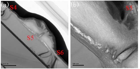
Figure 2435 shows an example of C, O, and Si contaminated bond pads. Area S6 had an abnormal film on the native Al oxide, while area S5 presented nonhomogeneous, loose and empty SixAlyCzOm materials in the hemispherical defect. These pad defects existed only at wafer edge because backside grinding was the root cause of the contamination.
Figure 2435. Contaminated bond pads. Adapted from [1]
However, in many cases, carbon is one of the most difficult contaminants, incorporated from fab-environment, to be detected by analytical TEM such as TEM-EDS and TEM-EELS techniques because of two reasons:
[1] Paul Yu, Jamie Su, Qiang Gao, Ming Li, Chorng Niou, Study of Aluminum Pad Contamination Sources during Wafer Fabrication, Shipping, Storage and Assembly, International Symposium on High Density packaging and Microsystem Integration, 2007. HDP '07.
|