Chapter/Index: Introduction | A | B | C | D | E | F | G | H | I | J | K | L | M | N | O | P | Q | R | S | T | U | V | W | X | Y | Z | Appendix
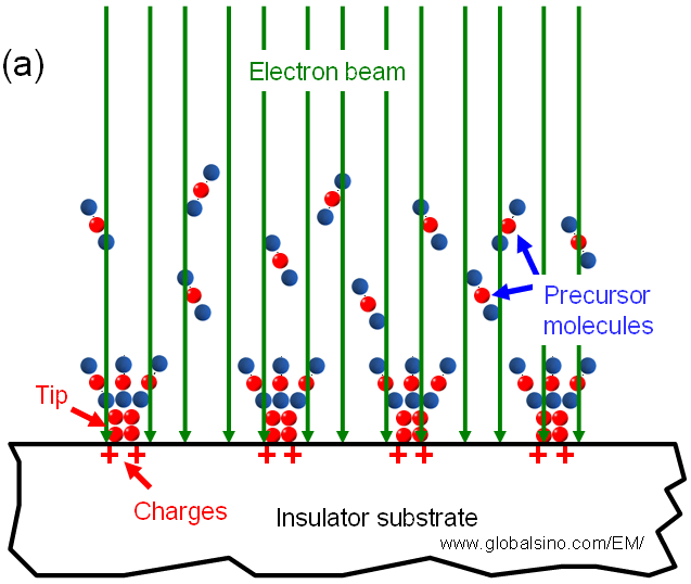
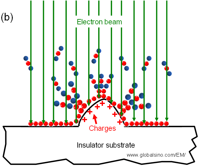
| The charge accumulation that enhances the growth rate of materials occurs often on an insulator substrate during electron beam induced deposition (EBID) and ion beam induced deposition (IBID). Figure 2498 shows the charging-enhanced growth mechanism during EBID. Under the incident electron irradiation, even though in the case that a flat substrate is used as shown in Figure 2498 (a), the distribution of the charges on the surface is still not uniform at a nanometer scale. The charges accumulated at some charge centers generate an electric field. Because the precursor molecules are easily polarized due to the weak bonding between the atoms of the molecules, the precursor molecules may be attracted to the charge centers on the surface. The molecules are then decomposed by the electron beam and form a deposit. Once the deposit is formed, the charges on the electrically conductive deposit tend to move and accumulate at the tip of the deposit. Therefore, the molecules are attracted to the tip, and the deposit increases in length upon further deposition. Figures 2498 (b) schematically show the preferential growth of materials on a non-flat surface of a substrate. In this case, the charges on the surface may move a long distance along the surficial deposits to the specific locations, e.g. the convex. And then, a strong electric field is formed near the convex surface. Therefore, the deposits grow preferentially on the convex surface because the charges attract polarized precursor molecules. For instance, nano-dendrites was formed on convex surfaces in EBID.
Figure 2498. Schematic illustration showing the process of EBID-induced growth of nanostructures with two different morphologies on insulating substrates. The red dots represent the deposit that is the nonvolatile fraction of the precursor, while the blue dots represent the volatile fraction of the precursor.
|