HRTEM and Diffraction of Gold (Au) Particles & Single Crystals - Practical Electron Microscopy and Database - - An Online Book - |
||||||||||||||||||||||||||||||||||||||||||||||||||||||||||||
| Microanalysis | EM Book https://www.globalsino.com/EM/ | ||||||||||||||||||||||||||||||||||||||||||||||||||||||||||||
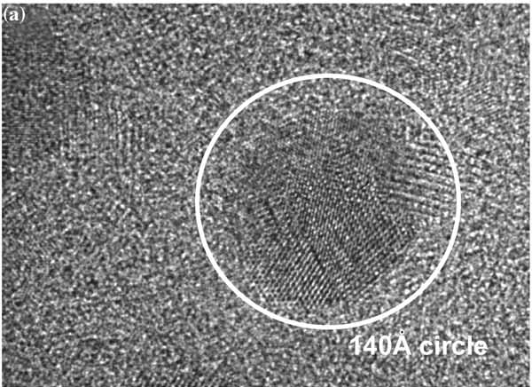
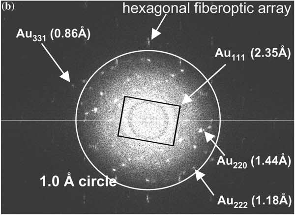
Figure 4171a (a) shows a HRTEM image of an Au particle on a very thin amorphous W/WO2 film and (b) shows that Fourier transformation of the image (a) produced diffractogram. The additional spots from hexagonal fiberoptic array in (b) were due to inadequate gain normalization.
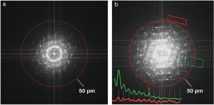
The extent of information transfer and the spatial resolution can be calculated by frequency space obtained from Young’s fringes produced by an image shift during imaging exposure. Figure 4171b shows the Fourier transforms of HRTEM (high-resolution TEM) images of gold (Au) nanoparticles on an amorphous carbon film. A monochromator was installed in the TEM system. When the monochromator was turned off, the Young’s fringes extended only to about 70 pm. When the monochromator was turned on and thus the effect of chromatic aberration was reduced, the Young’s fringes extended beyond 50 pm (red circle) in all directions, reflecting that this microscope with the monochromator has 50 pm spatial resolution.
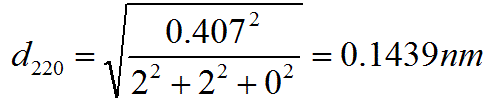
Crystal Au has cubic structure. Its lattice parameter is 0.407 nm so that the (220) lattice spacing (see page3547) can be given by, Table 4171 lists the angles (2θB) between the direct beam 000 and diffracted beams as well as the lattice spacings for Au at accelerating voltages of 100, 200, 300 and 400 kV.
[1] M. A. O’Keefe, C. J. D. Hetherington, Y. C. Wang, E. C. Nelson, J.H. Turner, C. Kisielowski, J. -O. Malm, R. Mueller, J. Ringnalda, M. Pane, and
A. Thust, Sub-Ångstrom high-resolution transmission electron microscopy at 300 keV, Ultramicroscopy 89 (2001) 215–241. |
|
|||||||||||||||||||||||||||||||||||||||||||||||||||||||||||
 ------------------- [4171]