=================================================================================
The lattice constants of cobalt silicides can be found elsewhere in the book. Figure 4491a shows planview TEM images and the corresponding indexed SAED (selected-area electron diffraction) patterns of (a and b) 400 °C, (c and d) 500 °C, and (e and f) 950 °C CoSix, formed by annealing Co/a-Si nanodot on SiGe substrate. The diffraction rings as marked in the three diffraction patterns were from polycrystalline CoSi2 and CoSi, respectively. The very bright diffraction spots in Figure 4491 (b) and (d) were from (0 0 1) SiGe substrate.
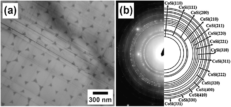
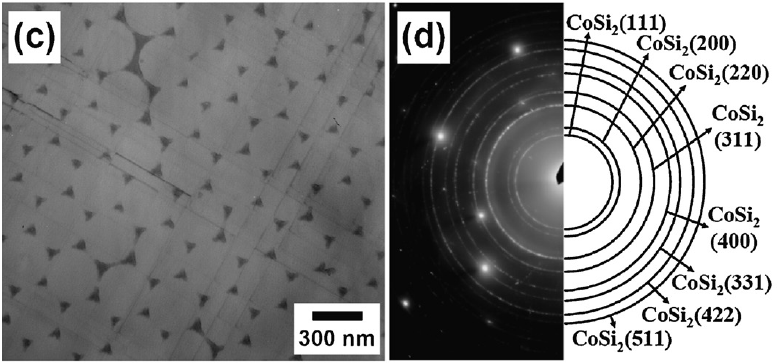
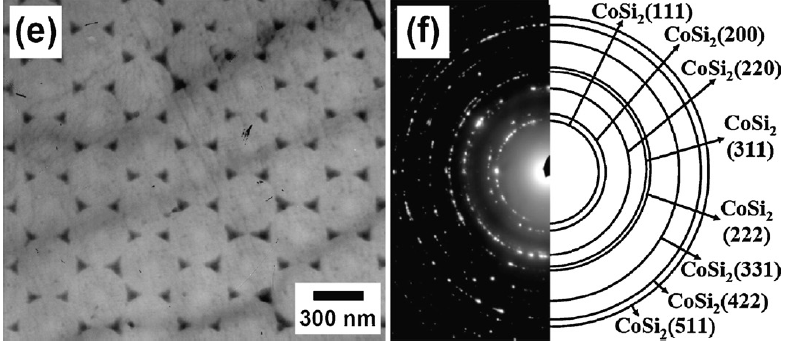
Figure 4491a. Planview TEM images and the corresponding indexed SAED patterns of (a and b) 400 °C,
(c and d) 500 °C, and (e and f) 950 °C annealed Co/a-Si nanodot samples [1].
Figure 4491b shows plan-view TEM image of the as-deposited CoSi2 film prepared from the composite target using a DC discharge power. The inset shows an electron diffraction pattern of the film. This film was perfectly amorphous without any nanocrystals.
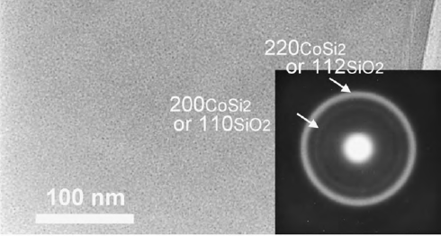
Figure 4491b. Diffraction pattern of amorphous CoSi2 film [2].
Figure 4491c shows the arrangement of atoms on CoSi2(200) (a) and CoSi(111) (b).
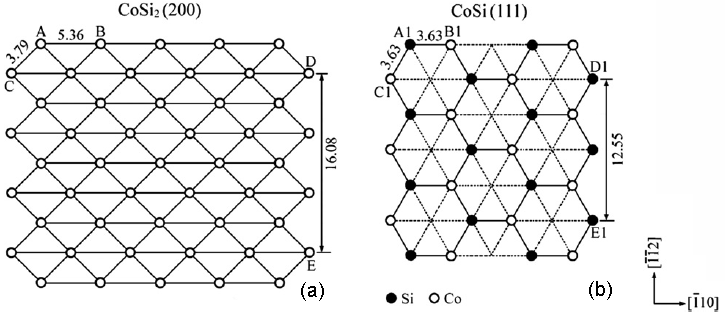
Figure 4491c. Arrangement of atoms on CoSi2(200) (a) and CoSi(111) (b) [3].
Figure 4491d shows indexed SAED patterns of 360 °C annealed Co(23 nm)/Au(4 nm)/(001) Si samples, where a mixture of CoSi2 and CoSi phases was formed after annealing.
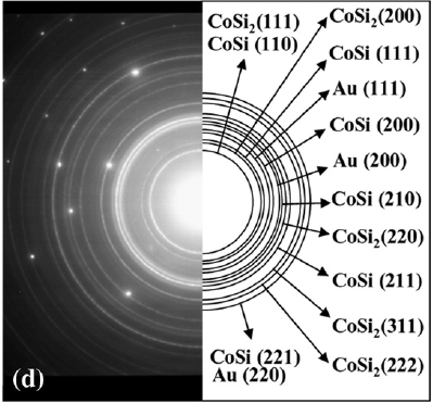
Figure 4491d. Indexed SAED patterns of 360 °C annealed Co(23 nm)/Au(4 nm)/(001) Si samples,
where a mixture of CoSi2 and CoSi phases was formed after annealing [4].
|
Table 4491. More diffraction patterns of cobalt disilicides.
| Cobalt disilicides |
Electron diffraction patterns |
| CoSi2 |
![SAED pattern along the [001] zone axis of CoSi2](image2/4491d.PNG)
SAED pattern along the [001] zone axis. [5] |
[1] Enhanced formation and morphological stability of low-resistivity CoSi2 nanodot arrays on epitaxial Si0.7Ge0.3 virtual substrate, S. L. Cheng, C.Y. Yang, S.W. Lee, H.F. Hsu, H. Chen, Materials Chemistry and Physics 130 (2011) 609– 614.
[2] Two routes to polycrystalline CoSi2 thin films by co-sputtering Co and Si,
Y. Tsuji, Y. Tsuji, S. Nakamura, and S. Noda, Applied Surface Science 256 (2010) 7118–7124.
[3] F. Zeng, X. Xiong, B. Huang, Cobalt silicide formations and magnetic properties of laser ablated Co(Cr) thin films, Intermetallics 18 (2010) 306–311.
[4] S.L. Cheng, H.Y. Chen, Effects of a thin Au Interlayer on the formation of low-resistivity CoSi2 on (001)Si substrate,
Thin Solid Films 516 (2008) 8797–8803
[5] Jaesang Lee, Keunwoo Lee, Dongock Kim, Taeyong Park, Honggyu Kim, and Hyeongtag Jeon, Epitaxial CoSi2 formation using an oxynitride buffer layer, J. Mater. Res., 24, 8, 2009.
|