Chapter/Index: Introduction | A | B | C | D | E | F | G | H | I | J | K | L | M | N | O | P | Q | R | S | T | U | V | W | X | Y | Z | Appendix
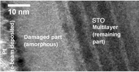
| The amorphized depth of silicon below the deposited Pt, by Ga ion beam, is between 30 and 50 nm in thickness. [2] As shown in Figure 4495, Pt deposition in the FIB system, prior to milling with the Ga beam induced amorphization of STO (SrTiO3) materials, even if the deposition is done by the electron beam (e-beam). The amorphized layer is more than 20 nm thick.
Figure 4495. Amorphization of STO induced by e-beam Pt deposition
[1]
[1] Montoya E, Bals S, Rossell MD, Schryvers D, and Tendeloo GV, Evaluation of Top, Angle, and Side Cleaned FIB Samples for TEM Analysis, Microscopy Research and Technique 70:1060–1071 (2007).
|