Chapter/Index: Introduction | A | B | C | D | E | F | G | H | I | J | K | L | M | N | O | P | Q | R | S | T | U | V | W | X | Y | Z | Appendix
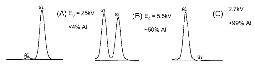
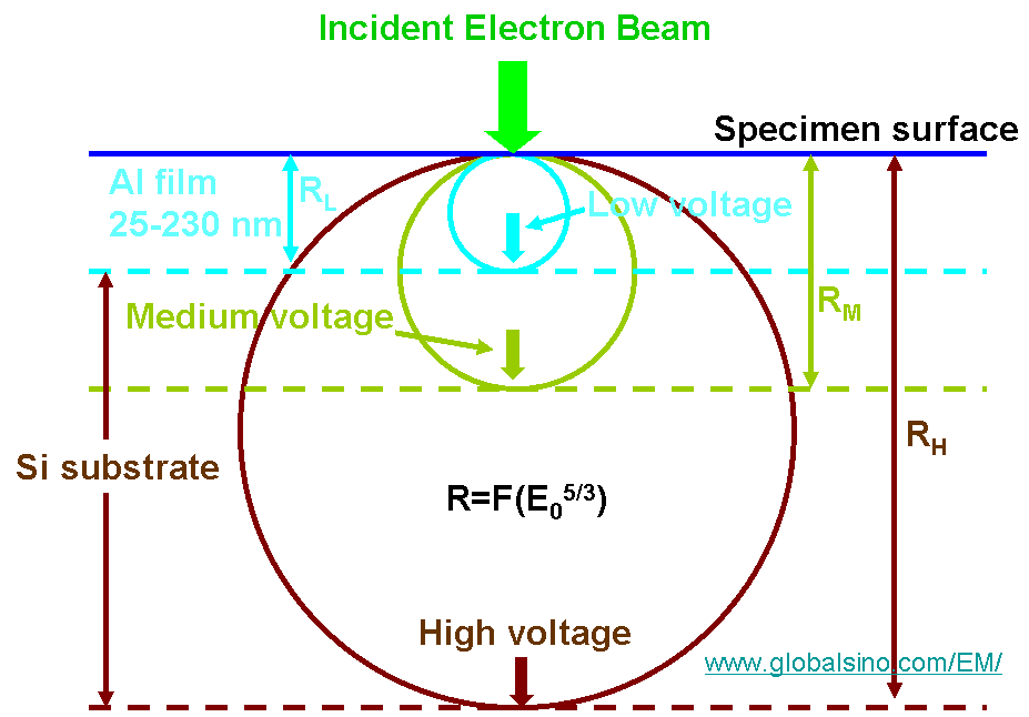
| Boyes [1] studied the emission behavior of low energy (<2 keV) X-rays from two-layer materials at low voltages (<6 keV) of the incident electron beams. A structure of aluminum (Al) deposited on silicon (Si) substrate was used in the investigation. The Al layer had thicknesses of 25 to 230 nm. Figure 4595a shows EDS spectra from a 104 nm Al film on the surface of a Si wafer as a function of the incident electron energy. At 25 kV of the incident electron beam, the Al film contributed signal of <4% in the total counts as shown in (A). At 5.5 kV the peak integrals from the thin film and the substrate are closely matched as shown in (B). At 2.7 kV the detected signal is almost exclusively (>99%) from the surface thin film as shown in (C), indicating at this energy the effective penetration of the electron beam into the bulk sample is restricted to a depth of less than 100 nm. These results can be explained by the interaction volume at different voltage of incident electron beam as indicated in Figure 4595b. The conclusion reminds us the emission of X-rays from different elements is strongly affected by the structure of the multiple layer materials and their stack sequence, and the energy of the incident electron beam.
Figure 4595a. EDS spectra from a 104 nm Al film on the surface of a Si wafer as a function of the incident electron energy (E0, kV).
[1] Edward D. Boyes, Analytical potential of EDS at low voltages, Mikrochim. Acta 138, 225-234 (2002).
|