Background Subtraction in EELS and EFTEM - Practical Electron Microscopy and Database - - An Online Book - |
||||||||
| Microanalysis | EM Book http://www.globalsino.com/EM/ | ||||||||
| ================================================================================= | ||||||||
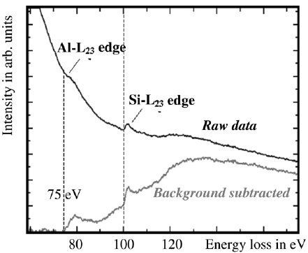
These characteristic ionization edges in EELS are superimposed on a background intensity due to zero-loss and plasmon peaks and the tails of edges lying at lower energies. The separation of energy loss signal from the background is necessary for extracting elemental information for elemental quantification and mapping. Due to the complexity of process contributing to the background, it is not possible to model the background from first principles. The method usually performed to calculate the background is to estimate the background contribution under the edge from the pre-edge area. The background can first be estimated and subsequently extrapolated to higher energies to subtract it from the core-loss region. Because of the similarities in signal extraction between EELS and EFTEM the same statistical extrapolation can be applied. Different methods for background subtraction have been proposed by numerous researchers [1 - 4]. Depending on the complexity of the chosen model, different number of filtered images at different energy losses in front of the core-edge has to be recorded according to the number of fitting parameters for the background subtraction. The EEL spectra in Figure 4723a show the Al L2,3 edge as well as the Si L2,3 edge after background subtraction, taken from AlxSiyOz matrix. Note that the background subtraction was done by referring to the first edge in the profile (Al L2,3 edge here).
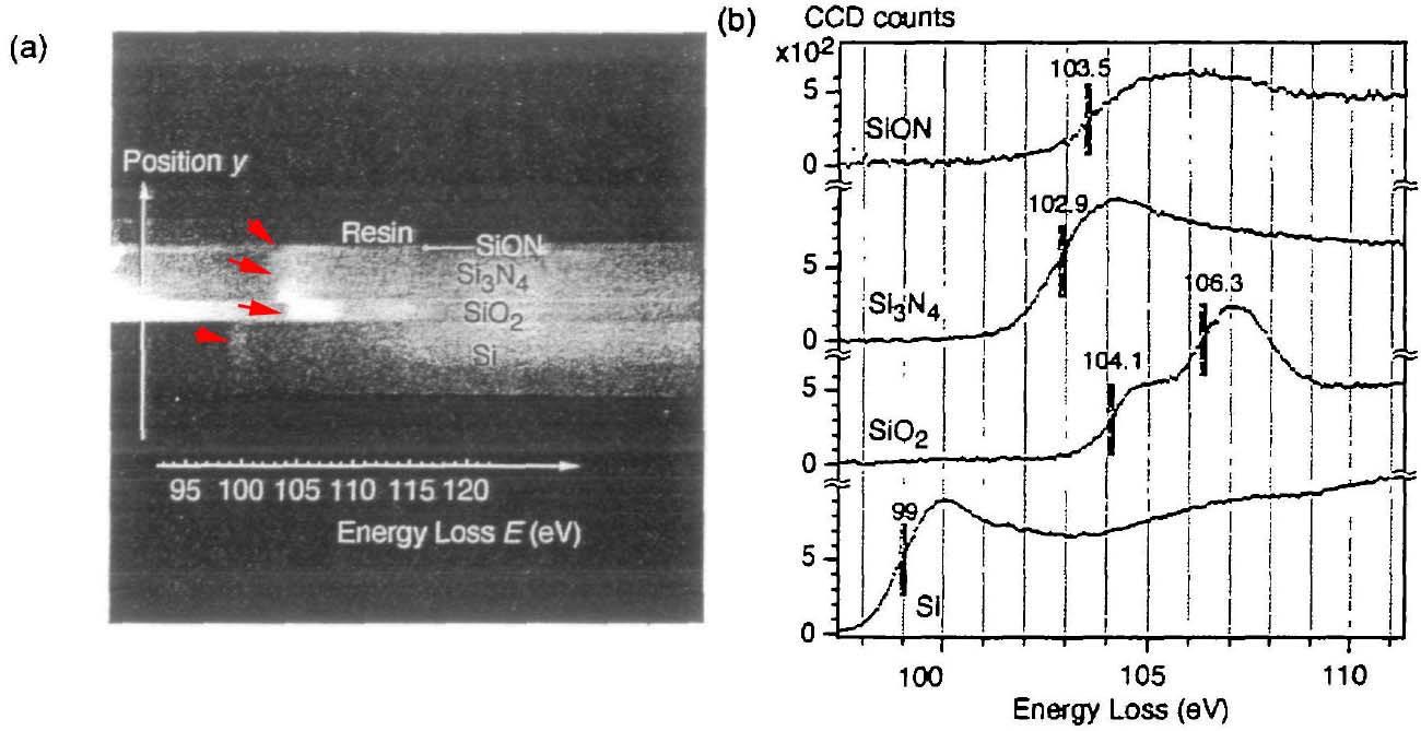
Figure 4723b shows that the chemical shifts are revealed by spatially resolved EELS of Si-L2,3 edges. Figure 4723b (a) shows the 2-D (two-dimensional) spectrum image obtained by an energy filter. Note that this image shows the image contrast before background subtraction. The vertical axis corresponds to the location (y) in the layered materials of SiON. Si3N4, SiO2 and pure Si. The horizontal axis corresponds to the energy loss E. Energy dispersion used here was 0.051 eV per pixel. The energy range ΔE recorded in the 2-D spectrum image was 52 eV (= 88 - 141 eV in energy loss). Both the shift of the bright lines (shown by red arrows) in Figure 4723b (a) and the vertical lines in Figure 4723b (b) indicate the chemical shift of Si-L2,3 edges. Figure 4723b (b) shows energy loss spectra of each layer extracted from Figure 4723b (a). Here, the backgrounds of the spectra were subtracted.
Figure 4723b. The spatially resolved EELS analysis of Si-L2,3 edges, (a) 2-D spectrum In EELS quantitative analysis, this background contribution Ib must be subtracted to obtain the core-loss signal Ik, The background (due mainly to the contribution of valence electrons) removal in EELS is much more different than in EDS because of the complexity and heterogeneity of the shape of the various edges. A couple of techniques have been proposed to subtract the background effects in EELS analysis and EFTEM mapping: Table 4723. Examples of background removal with inverse power-law model.
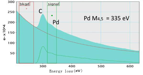
Figure 4723c shows an EEL spectrum, presenting Pd-M4,5 edge at 335 eV, taken from a Pd nanoparticle on holey carbon (C) film. Both the C and Pd signals are clear. In order to extract the Pd signal, the energy window for background subtraction is selected before the C K edge but not immediately before the Pd-M4 edge onset since there is uncertainty which is induced by the carbon peak.
In many cases, the background window cannot be too big since the energy peaks of other possible elements in the specimen are very close to the core-loss of the interesting element. For instance, for a core loss of the interesting element is about 348 eV, a small background window (e.g. 20 eV) is used to fit the spectrum in order to avoid the contribution from the carbon edge (284 eV), so that we only pick up the signal generated by the interesting element for the elemental evaluation. iii) The simplest approach of subtracting the background intensity in EFTEM elemental
maps is ratio mapping, where the post-edge intensity
Ipost is divided by the pre-edge intensity Ipre. If the shape of the background remains constant
across the entire image, then the ratio value k gives a simple representation of the distribution of an
element by,
[1] Bentley, J., Lehmann, G. L., Sklad, P. S., 1982. Alternative background
fitting for electron energy-loss spectra. In Proc. 40th Annual EMSA
|
||||||||
| ================================================================================= | ||||||||
|
|
||||||||