=================================================================================
Small fraction of incident electrons are scattered through large angles and the extreme case is 180° backscattering as shown in Figure 4755a. The scattering angle has been discussed in Section Elastic Scattering Angle of Electrons. In electron microscopes, a collection angle higher than 50 mrad allows acquisition of mainly incoherent electrons. The incoherent images are directly interpretable.
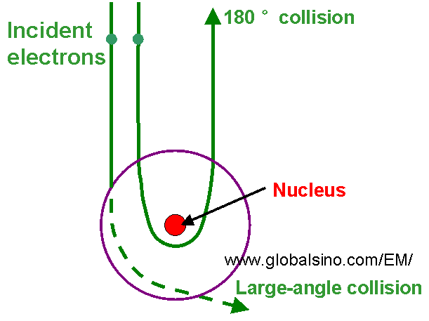
Figure 4755a. Elastic scattering of electrons from an atomic nucleus for a large-angle collision and a 180 ° collision.
Dark-field images in TEMs/STEMs are constructed using electrons scattered at relatively large (≥ 30 mrad for STEM) angles and are dominated by elastic and thermal diffuse scattering. Scattering in the range of high angles is dominated by Rutherford (elastic) scattering and thermal diffuse (quasi-elastically) scattering (TDS). Such scattering is very sensitive to the atomic number (Z) of the scattering atoms and therefore provides information of the local chemical composition [1]. The scattering cross section is proportional to Z2. In electron microscopic imaging, high-angle annular dark-field (HAADF) method is used to remove the complexity of conventional bright-field scattering in HRTEM and the associated diffraction complications.
In general, the higher the effective atomic number, the higher is
the inelastic differential cross-section. However, the ratio of the
inelastic to the elastic scattering cross-section is inversely
proportional to the effective atomic number, [3]
 ------------------------ [4755] ------------------------ [4755]
where,
σi --
the inelastic scattering cross-section,
σe --
the elastic scattering cross-section,
Zeff -- the effective atomic number,
C -- a coefficient,
 -- the characteristic angle corresponding to the mean energy loss. -- the characteristic angle corresponding to the mean energy loss.
Figure 4755b shows the angle at which inelastic and elastic differential cross-sections are equal, as a function of the atomic number Z at the energy loss of 10 eV.
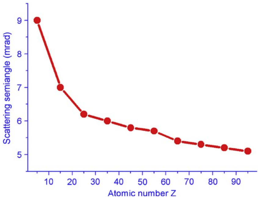
| Figure 4755b. Plot of the scattering angle at which elastic and inelastic differential cross-sections are equal, as a function of the atomic number at an energy loss of 10 eV. [2] |
[1] Characterization of III–V semiconductor interfaces by Z -contrast imaging, EELS and CBED, Hubert Lakner, Bernd Bollig, Stefan Ungerechts and Erich Kubalek, J. Phys. D: Appl. Phys. 29 1767–1778 (1996).
[2] Lin Gu, Wilfried Sigle, Christoph T. Koch, Jaysen Nelayah, Vesna Srot, Peter A. van Aken, Mapping of valence energy losses via energy-filtered annular dark-field scanning transmission electron microscopy, Ultramicroscopy 109 (2009) 1164–1170.
[3] A.V. Crewe, J.P. Langmore, M.S. Isaacson, Physical aspects of electron microscopy and microbeam analysis, in: B.M. Siegel, D.R. Beaman (Eds.),
Wiley, New York, 1975, p. 47.
|