| The principle of semiconductor detectors is based on solid-state physics.
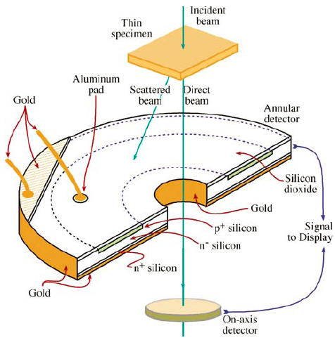 |
| Figure 4996 (a). Semiconductor detector of the surface-barrier type, shown in
a configuration where it would be used to detect high-energy, forward scattered
electrons (e.g. for TEM in this figure). The direct beam is detected by a small circular detector
on the optic axis of the microscope surrounded by a concentric wide-angle
annular detector (e.g. for HAADF imaging), which detects any scattered electrons. |
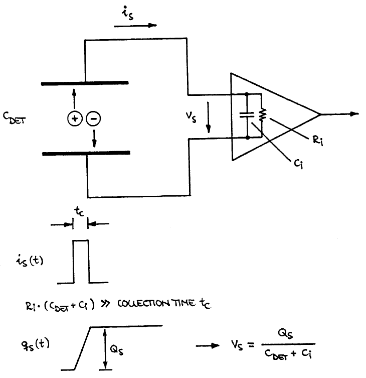 |
| Figure 4996 (b). Electron-hole pairs induce electrical current. |
The semiconductor detector, shown schematically in Figure 4996 (a), is a doped single-crystal sheet of Si (often
inaccurately described as a solid-state detector). We
make the Si into an electron-sensitive detector by creating
a p-n junction beneath the Si surface in one of two
ways. In one type of detector, we create the junction by
doping the Si (e.g., by ion implantation of n-type impurity
atoms into p-type Si or vice versa). This doping
disturbs the equilibrium charge carrier concentration
and creates a region across the p-n junction that is free
of majority carriers which we call a ‘depletion region.’ A
conducting metal layer is evaporated onto both surfaces
to provide ohmic contacts. The alternative type of detector
is called a surface-barrier detector (or sometimes a
Schottky diode) and we fabricate this by evaporating a
thin layer of Au on the surface of high-resistivity n-type
Si, or evaporating Al onto p-type Si. This surface layer
acts as an electrical contact and also creates a depletion
layer and a p-n junction just inside the Si. When we put either of these detectors into a beam of
high-energy electrons, most of the beam energy is transferred
to valence-band electrons in the Si which are
excited across the band gap into the conduction band
thus creating electron-hole pairs (see Figure 4996 (b)). We
can separate the electrons and holes most efficiently by
applying an external reverse bias to the detector; that is,
we put a negative bias on the p side of the junction and a
positive bias on the n side. In practice, however, so many
electron-hole pairs are created at TEM beam energies that an external bias is not usually necessary, and the
internal bias of the p-n junction acts to separate the
electrons and holes. Because the electrons and holes
move quite quickly in Si, it takes only a few nanoseconds
to gather most of the carriers over an area of ~ 1 µm2. So
the semiconductor detector is remarkably responsive to
electrons. The net result is that the incoming electron
signal is converted to a current in the external circuit
between the surface contacts, as shown in the surface barrier
detector in Figure 4996 (a).
Since it takes approximately 3.6 eV to produce an
electron-hole pair in Si at room temperature, a 100-keV
electron can theoretically produce ~28,000 electrons.
This represents a maximum detector gain of close to
3 x 10⁴ but in practice there are losses due to electron
absorption in the metal contact layer and recombination
of the electrons and the holes close to the Si surface
(in a region called the dead layer), and we actually get a
gain of closer to 2x10⁴.
These semiconductor detectors are very efficient at
picking up and amplifying electron signals. Unfortunately,
they have an inherently large capacitance, so
they are not very responsive to rapid changes in signal
intensity. Such changes are quite likely to occur during
the rapid scanning process of STEM imaging. In other
words, the detector has a narrow bandwidth (typically
100 kHz); this is not a good property for a detector which is subject to widely varying signal intensities.
We could lower the capacitance by decreasing the detector
area, but if we do this, the signal-to-noise ratio will
be lowered. It is the S/N ratio that ultimately limits the
quality of all scanning images.
Semiconductor detectors have several advantages
* We can easily fabricate them.
* They are cheap to replace.
* They can be cut into any shape, as long as it is flat.
This latter advantage makes them ideal for squeezing
into the confines of TEM stages and columns. For
example, we can make the semiconductor detector in
annular form so that the main electron beam goes
through the hole in it, but the scattered electrons are
very efficiently detected. This produces a dark-field
(scattered electron) detector. We can also make detectors
that are divided into halves or quadrants and each
segment is insulated from the other(s). These detectors
are very useful for discriminating directional signals
such as those coming from magnetic specimens.
There are also some drawbacks to semiconductor
detectors & They have a large dark current (the current registered
when no signal is incident on the detector).
This dark current arises from thermal activation of
electron-hole pairs, or from light falling on an uncoated detector. Since the detectors in a TEM
invariably have a metal ohmic contact, the light
problem is minimal because light can’t penetrate
the metal film.
Now we could minimize thermal
activation by cooling the detector to liquid-nitrogen
temperatures but that step is impractical and introduces
a cold surface into the vacuum which would
simply collect contamination, so we live with noise
due to the thermal activation.
* Because noise is inherent in the semiconductor
detector, its DQE is poor for low-intensity signals,
but rises almost to unity for high-intensity
signals.
* The electron beam can damage the detector, particularly
in intermediate voltage microscopes. In these
circumstances, a doped p-n detector is less sensitive
than a surface-barrier detector, because the depletion
region is deeper in the Si.
* They are insensitive to low-energy electrons such as
secondary electrons.
Despite these drawbacks, both types of Si detector
are far more robust than the alternative scintillator.
|
