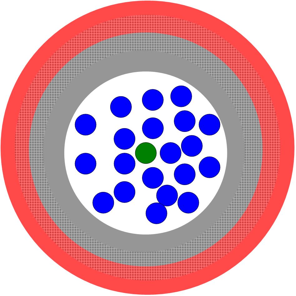
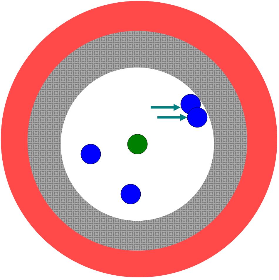
| Figure 1272a shows a diffraction pattern in STEM mode. This pattern contains three regions:
i) The diffraction pattern contains discs instead of spots since the electron beam is converged in STEM mode.
i.a) The green disc is the transmited beam.
i.b) The blue discs represent diffracted beams.
ii) The gray ring are "randomly" scattered electrons but not in a disc form, and is formed from elastical and quasi-elastical scattering at high angles between ~ 50 – 100 mrad and thus, contains only high-angle diffusely scattered electrons.
iii) The outer red ring shows electrons scattered at very high angles. Such scattered electrons are highly aberrated and distorted so that they are not good for STEM imaging.
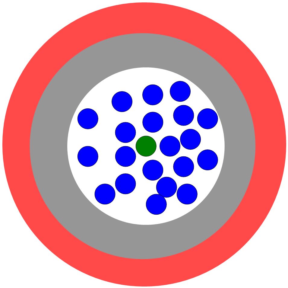
Figure 1272a. Diffraction pattern in STEM mode. |
We know that the sizes of the BF- and DF-detectors are fixed. Therefore, in principle, it is easy to understand that the transmitted electrons or different diffracted beams can be collected by moving the detectors (screen) down or up, as shown in Figure 1272b, which corresponds to the change of the camera length.
However, a couple of reasons make the detector movement impossible, for instance:
i) It is not convenient to mechanically move the detectors up and down in a vacuum condition.
ii) The proper camera lengths for different applications can be from cm to 30 m. The vacuum column does not such a wide room to move the detectors.
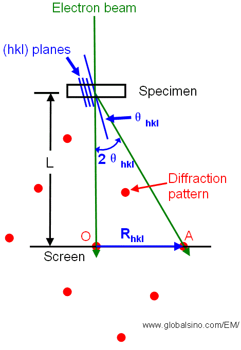
| Figure 1272b. Relationship between the reciprocal lattice spacing Rhkl and the camera length L for diffraction in a TEM. |
However, instead of moving the detectors up and down to select and record the intensities of the transmitted and/or different diffracted beams, we can conveniently change the lens currents to zoom in (magnify) or zoom out (demagnify) the diffraction pattern on the detectors. This zoom-in and zoom-out process, in fact, decreases and increases the effective distance between the specimen and the detector, respectively, and thus, is then converted to the corresponding camera lengths on the commercial microscopes. Therefore, the collection angles of the detector can be varied simply by changing the effective camera length.
Even though electron diffraction (e.g. µ-diff and CBED) can be recorded with cameras, it is important to know that the signals collected by STEM detectors or GIF camera for EELS are the scattered electrons in one or more regions (rings or discs) in Figure 1272a. Note that the GIF camera here acts as a detector as well, that is, it collects all the electrons which fall into the camera and outputs a signal as a single intensity but do not sort the electrons by diffraction spots, similar to STEM detectors. Depending on the selection of scattered electrons, we have the main applications listed in Table 1272.
| Table 1272. Main applications with various selections of the scattered electrons (mainly arranged from the smallest to largest camera length). |
| Camera length |
Used region in STEM diffraction pattern |
Detector or camera used |
Names |
Applications |
| Perfect system |
Imperfect system |
| Very small (e.g. 7.7 cm) |
All the patterns smaller than the gray ring |
Full green disc and partial white ring are used |
GIF camera acts a detector |
EELS |
EELS measurement |
| Very small (4 - 10 cm) |
Gray ring |
|
Angle annular dark field detector |
HAADF |
Collects high-angle scattering incoherent electrons and presents Z-contrast from composition but eliminates diffraction contrast, and thickness determination. |
| Small (e.g. 10 to 200 cm) |
|
|
CCD camera |
Diffraction |
Observation of HOLZ lines and Kossel patterns, and selected area diffraction pattern |
| Small |
All the patterns smaller than the red ring |
|
CCD camera |
CBED |
Crystal structure and symmetry (page2694) |
| Medium (e.g. 40 cm) |
|
|
CCD camera |
Diffractions |
Kickuchi lines |
| Large |
White ring with blue discs |
|
Angle annular dark field detector |
ADF |
Deformation strain and subgrains can be observed due to diffraction effects (contrast) |
| Very large (e.g. 60 cm) |
Green disc only (Figure 1272c) |
Partial green disc is used, or full green disc and partial white ring are used |
Bright field detector |
Bright field |
Bright field imaging |
| Very large |
|
|
CCD camera |
CBED or diffraction |
Study the details of single or few diffraction spots or discs |
| Green disc only |
|
CCD camera |
CBED |
Crystal structure and symmetry (page2694) |
| |
CCD camera |
|
Kossel-Möllenstedt (K-M) fringes, HOLZ sharp dark lines in BF disc |
| Extremely large |
Green disc partially |
|
Angle annular dark field detector |
ABF |
Collects coherent electrons with scattering angles from ~10 to ~20 mrad, which is equivalent to the hollow-cone illumination in TEM mode |
| Others related to camera length: |
| Larger |
|
|
Angle annular dark field detector |
ADF |
Maximize the signal on the annular detector |
| Larger |
|
|
CCD camera |
Diffraction |
Avoid oversaturating the CCD camera, e.g. at high probe currents used in EDS |
| Any |
None |
|
EDS detector |
EDS |
EDS measurement |
* ADF: angle annular dark field.
HAADF: High angle annular dark field.
ABF: Annular bright-field |
In correct BF-STEM imaging, a bright field STEM detector is inserted as shown by the red circle in Figure 1272c. In this case, the intensity of the STEM image is determined by the transmitted disc only, but the intensities of the other discs are not collected by the detector. Note that the collected intensity depends on crystal orientations, for instance, the detector collects less electrons if more electrons are diffracted into the diffration discs at a specific crystalline orientation.
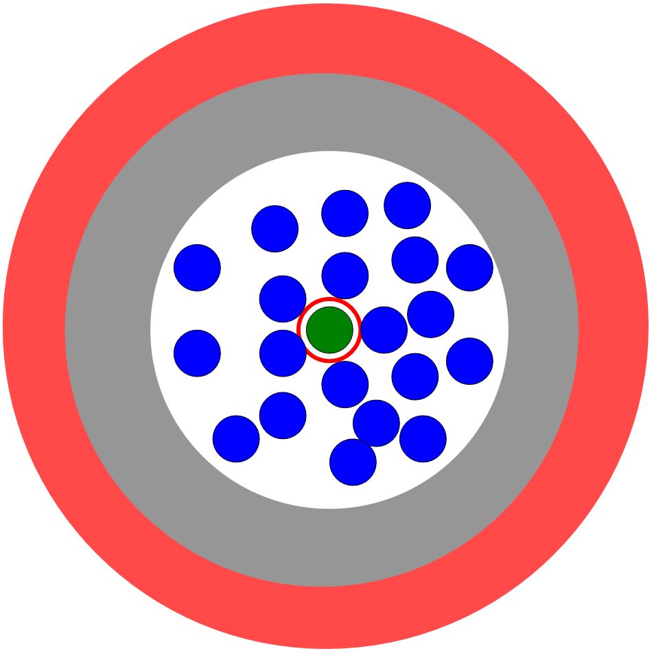
Figure 1272c. BF(bright field)-STEM imaging. |
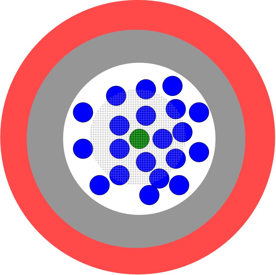
As indicated in Table 1272, the best acceptance of the EEL spectrometer is that the spectrometer collects all the electrons in the patterns smaller than the gray ring as shown in Figure 1272a. However, in reality, the acceptance is often much smaller than the range which needs to be collected because of lack of compatibility between STEM detector and EELS spectrometer in their physical configurations:
i) When the spectrometer is able to collect all the electrons in the patterns smaller than the gray ring as shown in Figure 1272d (a), the STEM detector is using the scattered electrons in the dashed area to form images. This is an unfavorite condition since the dashed area contains some distorted rays in red but only the scattered electrons in gray area partially. Unfortunately, this is a very common condition if you only use STEM detectors from microscope manufacturers.
ii) When the STEM detector is able to record images in good quality (the scattered electrons in the gray region, i.e. HAADF condition), the EEL spectrometer only collects the diffracted electrons partially as shown in Figure 1272d (b).
Figure 1272d. Non-ideal combinations of the STEM detector and EEL spectrometer: (a) The spectrometer has its proper camera length, that is, it records all the transmitted and diffracted electrons in the white region, but the STEM detector records the electrons in dashed regions and thus does not have good imaging-quality, and (b) The STEM detector has its proper camera length, but the spectrometer records the electrons in the dashed regions and thus does not have the strongest signal or good quality. |
There is an EELS measurement artifact when the second non-ideal condition in Figure 1272d is used. For instance, in the structure in Figure 1272d (a), even though the content of element X in yellow at location B is higher than or equals to that in blue at location A, the EELS elemental map still shows that location A has a higher amount of element X than location B because the diffracted rays in yellow (in Figure 1272e (b)) from location B (in Figure 1272e (a)) are not recorded by the EEL spectrometer.
Figure 1272e. (a) Structure mapped with EELS and STEM techniques, and (b) Diffracted beams at locations A and B. Both locations A and B in (a) have the same amount of element X, but their crystalline orientations are different so that their diffraction pattern in (b) are different. The diffracted beams in yellow in (b) are from location B in yellow in (a), while the diffracted beams in blue in (b) are from location A in blue in (a).
|
Fortunately, Gatan provides its own STEM detectors which can be installed and simultaneously set to desired values with the spectrometer by setting the projector lenses to obtain a proper camera length. That is, the spectrometer can collect all the scattered electrons in the white area and the STEM detector can use all the diffusely scattered electrons in the gray area in Figure 1272a. In this way, both the spectrometer and STEM detector are working in an ideal condition.
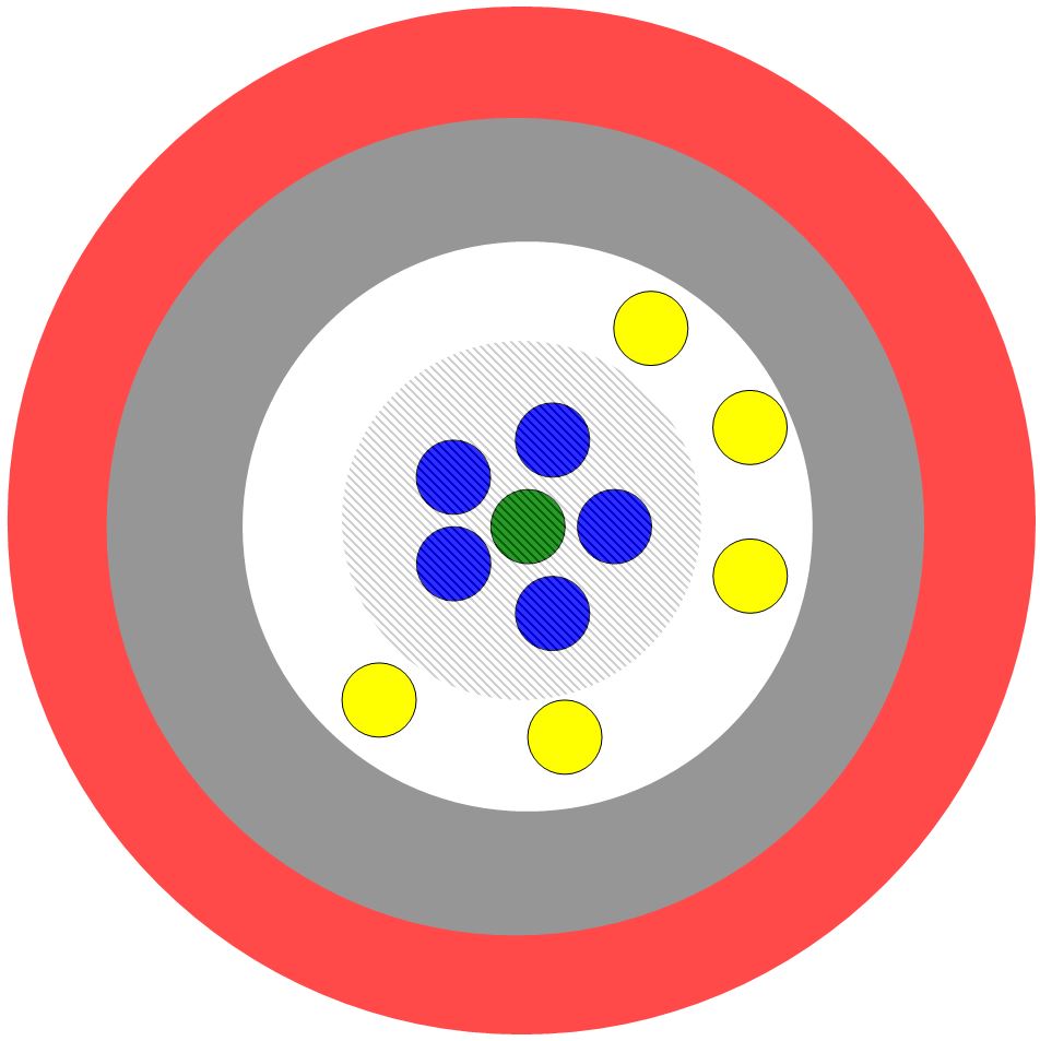
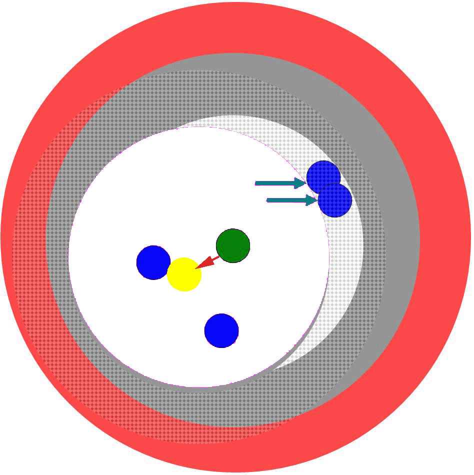
Figure 1272f shows that the specific diffracted discs, marked by the two green arrows, can be selected for STEM imaging by shifting projector lens alignment (PLA) in the direction marked by the red arrow, so that the grains in such particular crystalline orientations can be highlighted in the DF-STEM images.
Figure 1272f. (a) The center of ADF STEM detector is at the transmitted beam and the recorded signal is from the dashed area (exactly the gray ring), and (b) The center of ADF STEM detector is shifted to the yellow disc in the direction marked by the red arrow and thus the two diffracted discs marked by the two green arrows are included in the recorded signal in the dashed area.
|
Note that the electron wavelength used in electron microscopes is shorter when a higher voltage is applied, then longer camera length is needed to produce a convenient diffraction pattern for recording.
|