
Chapter/Index: Introduction | A | B | C | D | E | F | G | H | I | J | K | L | M | N | O | P | Q | R | S | T | U | V | W | X | Y | Z | Appendix
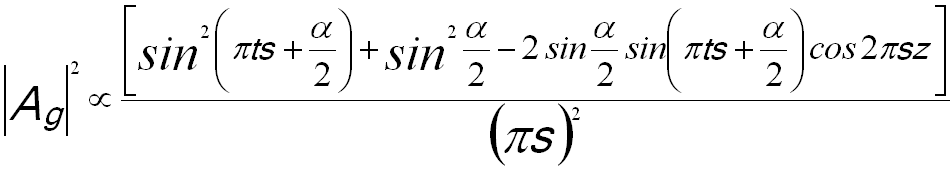
| In kinematic approximation, by introducing a phase shift (α) at a stacking fault, the TEM imaging intensity (|Ag|2) is given by, Equation 1996a indicates that the visibility of the stacking fault is dependent on α, s, and z. Figure 1996 shows stacking faults in the silicon substrate, which are defects where the normal stacking sequence of atomic planes is disrupted. These types of defects can have a significant impact depending on their proximity to device features, such as the source and drain regions of a transistor. If a stacking fault crosses a p-n junction, it can increase leakage current across the junction, potentially causing device failure.
[1] Raghaw S. Rai and Swaminathan Subramanian, Role of transmission electron microscopy in the semiconductor industry for process development and failure analysis, Progress in Crystal Growth and Characterization of Materials, 55, pp.63-97, 2009.
|
 -------------------- [1996a]