| FIB sputtering is a pure physical collision process between ions and substrate. It works with low ion energies (e.g. ≤50 keV) because the effect of implantation in FIB should be as little as possible. Ionic sputtering yield is the ratio of the number of the target atoms (or molecules) ejected from the target to the number of ions incident on the target surface, i.e., atoms sputtered per incoming ion. The yield depends on many factors, including ion mass, ion energy, atomic mass of the target, and the crystallinity of the sample. For each material there exists a threshold energy below which no sputtering occurs. This energy is normally in the range of 10 to 30 eV.
Many materials such as Al, Cu, Zn, Si, and SiO2 have the highest sputtering yields at angles in the range of 75° to 85°. Figure 2455a shows the schematic illustration of relative sputtering yield against the angle of incidence with respect to target normal. For instance, the sputtering yields of Si and SiO2 are about 6 to 7 times larger than that at the zero angle.
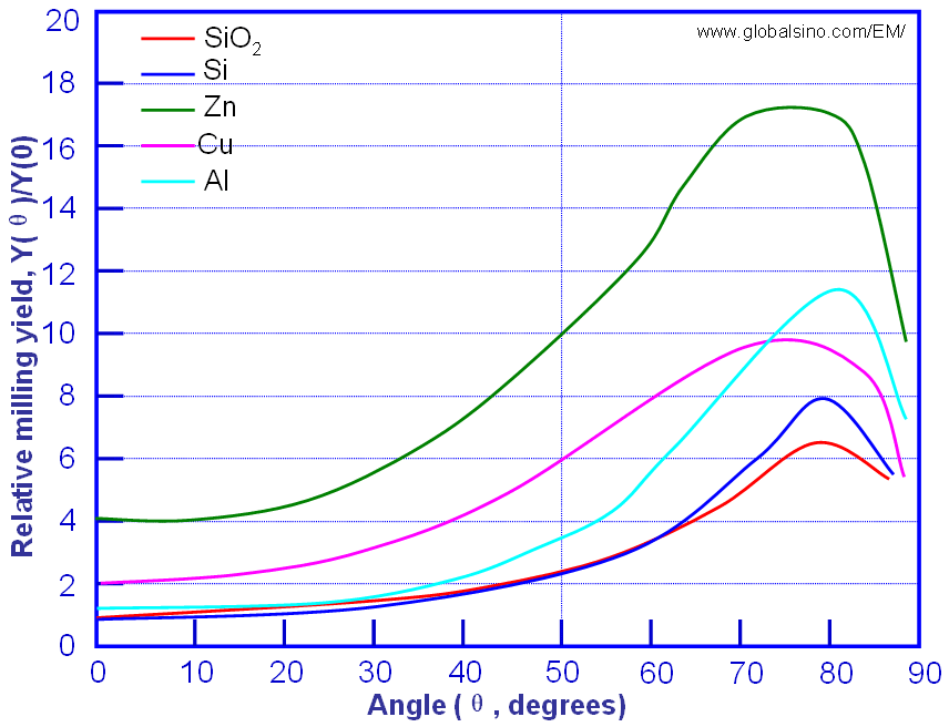
Figure 2455a. Schematic illustration of ionic sputtering yield against the angle (θ) of incidence with respect to target normal.
Figure 2455b shows the dependence of ionic sputtering yields on the energies of different ions in the energetic beams. Here, the incident ions (Au, Nd, In, Ga, Co, Si, N, and Li) are normal to the silicon (Si) target surface. In FIB, the ions in the energetic beam are normally Ga+ ions.
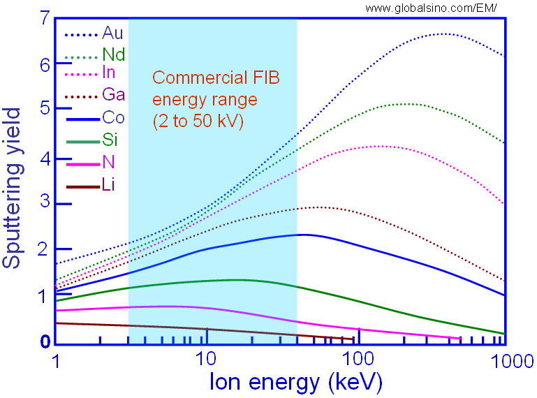
Figure 2455b. The dependence of ionic sputtering yields on ion energies. The target material is silicon.
Figure 2455c shows the sputtering yield of a FIB as a function of beam-ion mass at 30 keV with a normal incidence on silicon target.
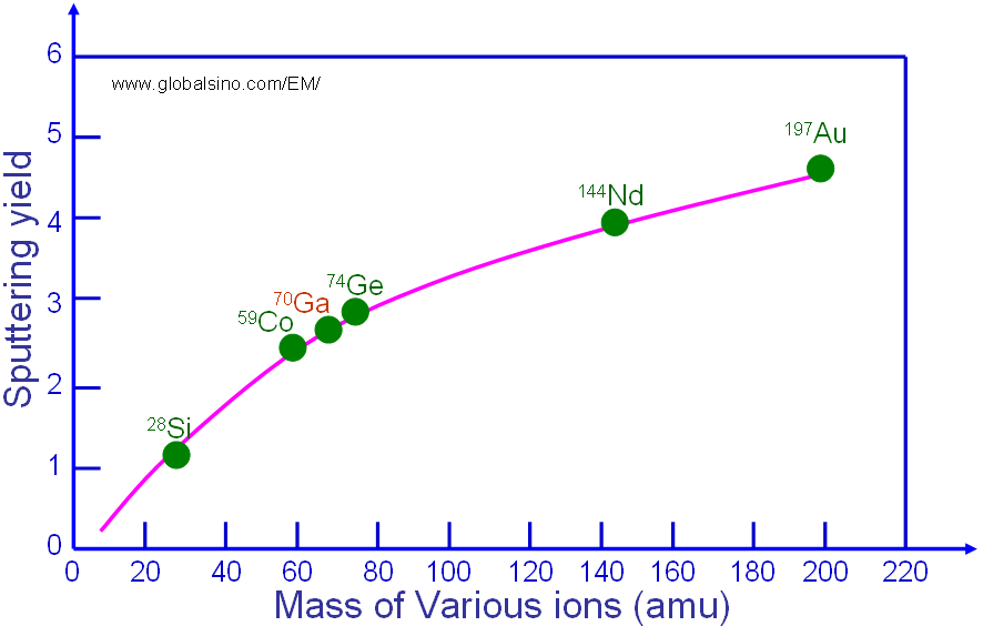
Figure 2455c. The sputtering yield of a FIB as a function of beam-ion mass at 30 keV with a normal incidence on Si target.
Positive and negative SIMS yields are significantly improved by using O2+ and Cs+ primary beams, respectively. These beams provide chemical reactions with the surface, which increases the ion yield. Figure 2455d shows the secondary ion yields for O2+ primary beam.
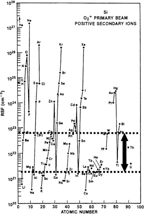
Figure 2455d. Secondary ion yields for O2+ primary beam. [10]
Table 2455. Examples of milling yields and rates of different materials in FIB. The incident angle is the angle of incidence with respect to target normal.
Table 2455a. Examples of milling yields and rates of different materials in FIB at the ion beam energy of 30 kV at the incident angle of 0°. Actual sputter rates can depend on lateral size and
aspect ratio of a structure or the crystal orientation of the substrate material. |
| Primary ion |
Ga+ |
Al+ |
In+ |
| Sputter yield/rate |
Sputter yield
(atoms/ion) |
Sputter rate
(µm3/nC) |
Sputter yield
(atoms/ion) |
Sputter rate
(µm3/nC) |
Sputter yield
(atoms/ion) |
Sputter rate
(µm3/nC) |
| AlAs |
|
0.30 - 0.42 [8] |
|
|
|
|
| Al3O2 |
|
0.0333 - 0.1 |
|
|
|
|
| Brass |
|
0.30 |
|
|
|
|
| Bronze |
|
0.20 |
|
|
|
|
| C (diamond) |
2.73 |
0.02 - 1.8 [4, 5] |
|
|
|
|
| Fe2O3 |
|
0.25 |
|
|
|
|
| GaAs |
|
0.61-0.89 |
|
|
|
|
| GaN |
6.1 (50 scans) - 6.26 (10 scans) [2] |
0.422 (50 scans) - 0.435 (10 scans) [2] |
|
|
|
|
| InAs |
|
1.10 - 1.40 [8] |
|
|
|
|
| InP |
|
0.96 - 1.2 |
|
|
|
|
| LiNbO3 |
|
0.07 - 0.35 |
|
|
|
|
| MgO |
|
0.15 |
|
|
|
|
| Nb-Pt1−xNix-Nb-Pt1−xNix multilayers |
|
0.235 - 0.296 [9] |
|
|
|
|
| PMMA |
|
0.40 - 0.50 |
|
|
|
|
| 6H SiC |
|
0.15 [2] |
|
|
|
|
| SiO2 |
|
0.19-0.24 |
|
|
|
|
| SiO2 (thermal) or TEOS |
|
0.24 |
|
|
|
|
| Si3N4 |
|
0.16-0.21 |
|
|
|
|
| Stainl. Steel |
|
0.32 |
|
|
|
|
| TiO |
|
0.15 |
|
|
|
|
| TiN |
|
0.15 |
|
|
|
|
| Vitreous ice |
|
5 |
|
|
|
|
| W nanowires |
|
~ 0.60 [3] |
|
|
|
|
| Biological Cells |
|
2 [7] |
|
|
|
|
| 1 |
H |
|
|
|
|
|
|
| 2 |
He |
|
|
|
|
|
|
| 3 |
Li |
|
|
|
|
|
|
| 4 |
Be |
|
|
|
|
|
|
| 5 |
B |
|
|
|
|
|
|
| 6 |
C |
|
0.18 |
|
|
|
|
| 7 |
N |
|
|
|
|
|
|
| 8 |
O |
|
|
|
|
|
|
| 9 |
F |
|
|
|
|
|
|
| 10 |
Ne |
|
|
|
|
|
|
| 11 |
Na |
|
|
|
|
|
|
| 12 |
Mg |
|
|
|
|
|
|
| 13 |
Al |
2.89 |
0.29-0.37 |
|
|
|
|
| 14 |
Si |
2.08-2.1 |
0.15-0.27 |
0.9 |
0.11 |
2.9 |
0.36 |
| 15 |
P |
|
|
|
|
|
|
| 16 |
S |
|
|
|
|
|
|
| 17 |
Cl |
|
|
|
|
|
|
| 18 |
Ar |
|
|
|
|
|
|
| 19 |
K |
|
|
|
|
|
|
| 20 |
Ca |
|
|
|
|
|
|
| 21 |
Sc |
|
|
|
|
|
|
| 22 |
Ti |
3.35 |
0.37-0.46 |
|
|
|
|
| 23 |
V |
|
|
|
|
|
|
| 24 |
Cr |
1.20 |
0.09-0.28 |
|
|
|
|
| 25 |
Mn |
|
|
|
|
|
|
| 26 |
Fe |
|
0.29 |
|
|
|
|
| 27 |
Co |
|
|
|
|
|
|
| 28 |
Ni |
|
0.14 |
|
|
|
|
| 29 |
Cu |
1.8 |
0.13-0.25 |
0.9 |
0.07 |
5.2 |
0.39 |
| 30 |
Zn |
3.57 |
0.34 |
|
|
|
|
| 31 |
Ga |
|
|
|
|
|
|
| 32 |
Ge |
1.55 |
0.22 |
|
|
|
|
| 33 |
As |
|
|
|
|
|
|
| 34 |
Se |
2.52 |
0.43 |
|
|
|
|
| 35 |
Br |
|
|
|
|
|
|
| 36 |
Kr |
|
|
|
|
|
|
| 37 |
Ru |
|
|
|
|
|
|
| 38 |
Sr |
|
|
|
|
|
|
| 39 |
Y |
|
|
|
|
|
|
| 40 |
Zr |
2.5 |
0.36 |
1.2 |
0.18 |
1.9 |
0.28 |
| 41 |
Nb |
|
|
|
|
|
|
| 42 |
Mo |
1.1-1.32 |
0.10-0.12 |
0.8 |
0.07 |
2.0 |
0.19 |
| 43 |
Tc |
|
|
|
|
|
|
| 44 |
Ru
|
|
|
|
|
|
|
| 45 |
Rh |
|
|
|
|
|
|
| 46 |
Pd |
|
|
|
|
|
|
| 47 |
Ag |
0.94 |
0.42 |
|
|
|
|
| 48 |
Cd |
|
|
|
|
|
|
| 49 |
In |
|
|
|
|
|
|
| 50 |
Sn |
1.17 |
0.25 |
|
|
|
|
| 51 |
Sb |
|
|
|
|
|
|
| 52 |
Te |
|
|
|
|
|
|
| 53 |
I |
|
|
|
|
|
|
| 54 |
Xe |
|
|
|
|
|
|
| 55 |
Cs |
|
|
|
|
|
|
| 56 |
Ba |
|
|
|
|
|
|
| 57 |
La |
|
|
|
|
|
|
| 58 |
Ce |
|
|
|
|
|
|
| 59 |
Pr |
|
|
|
|
|
|
| 60 |
Nd |
|
|
|
|
|
|
| 61 |
Pm |
|
|
|
|
|
|
| 62 |
Sm |
|
|
|
|
|
|
| 63 |
Eu |
|
|
|
|
|
|
| 64 |
Gd |
|
|
|
|
|
|
| 65 |
Tb |
|
|
|
|
|
|
| 66 |
Dy |
|
|
|
|
|
|
| 67 |
Ho |
|
|
|
|
|
|
68
|
Er |
|
|
|
|
|
|
69
|
Tm |
|
|
|
|
|
|
70
|
Yb |
|
|
|
|
|
|
71
|
Lu |
|
|
|
|
|
|
72
|
Hf |
|
|
|
|
|
|
73
|
Ta |
3.5 |
0.32-0.40 |
1.3 |
0.15 |
2.0 |
0.22 |
74
|
W |
1.1-1.22 |
0.11-0.12 |
0.8 |
0.08 |
2.1 |
0.21 |
75
|
Re |
|
|
|
|
|
|
76
|
Os |
|
|
|
|
|
|
77
|
Ir |
|
|
|
|
|
|
78
|
Pt |
2.44 |
0.23 |
|
|
|
|
79
|
Au |
|
1.5-1.8 |
|
|
|
|
80
|
Hg |
|
|
|
|
|
|
81
|
Tl |
|
|
|
|
|
|
82
|
Pb |
|
2.87 |
|
|
|
|
83
|
Bi |
|
|
|
|
|
|
84
|
Po |
|
|
|
|
|
|
85
|
At |
|
|
|
|
|
|
86
|
Rn |
|
|
|
|
|
|
87
|
Fr |
|
|
|
|
|
|
88
|
Ra |
|
|
|
|
|
|
89
|
Ac |
|
|
|
|
|
|
90
|
Th |
|
|
|
|
|
|
| 91 |
Pa |
|
|
|
|
|
|
| 92 |
U |
|
|
|
|
|
|
| Reference |
|
|
|
|
|
|
Table 2455b. Other examples of milling yields and rates of different materials in FIB.
| Sputtered material |
Milling rate
(µm3nC-1) |
Total Yield (Atoms/Ion) |
| Beam energy: 70 kV; Ion beam: Ga+; Incident angle*: 30° |
| GaN |
0.577 (10 scans) - 0.592 (50 scans) [2] |
8.33 (10 scans) - 8.5 (50 scans) [2] |
| Beam energy: 70 kV; Ion beam: Ga+; Incident angle: 15° |
| GaN |
0.512 (10 scans) - 0.541 (50 scans) [2] |
7.4 (10 scans) - 7.7 (50 scans) [2] |
| Beam energy: 70 kV; Ion beam: Au++; Incident angle: 0° |
| Si |
0.61 [6] |
|
| SiC |
0.32 [6] |
|
| Beam energy: 70 kV; Ion beam: Co++; Incident angle: 0° |
| Si |
0.305 [6] |
|
| SiC |
0.07 [6] |
|
| Beam energy: 70 kV; Ion beam: Ga+; Incident angle: 0° |
| Al3O2 |
0.13 |
|
| GaN |
0.451 (10 scans) - 0.47 (50 scans) [2] |
6.5 (10 scans) - 6.75 (50 scans) [2] |
| Si |
0.28 |
|
| 6H SiC |
0.15 |
|
| Beam energy: 70 kV; Ion beam: Ge++; Incident angle: 0° |
| Si |
0.33 [6] |
|
| SiC |
0.12 [6] |
|
| Beam energy: 70 kV; Ion beam: Nd ++; Incident angle: 0° |
| Si |
0.53 [6] |
|
| SiC |
0.2 [6] |
|
| Beam energy: 50 kV; Ion beam: Ga+; Incident angle: 30° |
| GaN |
0.577 (10 scans) - 0.6 (50 scans) [2] |
8.3 (10 scans) - 8.7 (50 scans) [2] |
| Beam energy: 50 kV; Ion beam: Ga+; Incident angle: 15° |
| GaN |
0.51 (10 scans) - 0.54 (50 scans) [2] |
7.3 (10 scans) - 7.8 (50 scans) [2] |
| Beam energy: 50 kV; Ion beam: Ga+; Incident angle: 0° |
| Al3O2 |
0.13 |
|
| GaN |
0.45 [2] |
6.8 [2] |
| Si |
0.264 |
|
| 6H SiC |
0.145 |
|
| Beam energy: 30 kV; Ion beam: Ga+; Incident angle: 30° |
| GaN |
0.576 (10 scans) - 0.598 (50 scans) [2] |
8.3 (10 scans) - 8.6 (50 scans) [2] |
| Beam energy: 30 kV; Ion beam: Ga+; Incident angle: 15° |
| GaN |
0.51 (10 scans) - 0.536 (50 scans) [2] |
7.3 (10 scans) - 7.71 (50 scans) [2] |
| Beam energy: 25 kV; Ion beam: Ga+; Incident angle: 0° |
| Cu |
0.7 [1] |
|
| Beam energy: 25 kV; Ion beam: Ga+; Incident angle: 12° |
| Cu |
1.13 [1] |
|
| Beam energy: 15 kV; Ion beam: Ga+; Incident angle: 30° |
| GaN |
0.55 [2] |
7.9 [2] |
| Beam energy: 15 kV; Ion beam: Ga+; Incident angle: 15° |
| GaN |
0.43 [2] |
6.2 [2] |
| Beam energy: 15 kV; Ion beam: Ga+; Incident angle: 0° |
| GaN |
0.362 [2] |
5.2 [2] |
| Beam energy: 5 kV; Ion beam: Ga+; Incident angle: 0° |
| Biological Cells |
0.6 [7] |
|
| * The angles are the angles from normal incidence. |
[1] Microelectronic Failure Analysis Desk Reference: 2001 Suppplement.
[2] A. J. Steckl and I. Chyr, Focused ion beam micromilling of GaN and related substrate materials (apphire, SiC, and Si…), J. Vac. Sci. Technol. B 17(2), 362 (1999).
[3] Wuxia Li, Ajuan Cui, Changzhi Gu, P. A. Warburton, Atomic resolution top-down nanofabrication with low-current focused-ion-beam thinning, https://doi.org/10.1016/j.mee.2012.07.108.
[4] S. Reyntjens and R. Puers, J. Micromech. Microeng., 11, 287 (2001).
[5] Rustin Golnabi, Won I. Lee, Deok-Yang Kim, and Glen R. Kowach, Mater. Res. Soc. Symp. Proc. Vol. 1282. 111 (2011).
[6] Lothar Bischofl and Jochen Teichert, Focused Ion Beam Sputtering of Silicon and Related Materials, Research Center Rossendorf Inc., Institute of Ion Beam Physics and Materials Research, Germany.
[7] http://www.anff.org.au/case-studies/focused-ion-beam-milling-biological-cells.html.
[8] K. A. Grossklaus and J. M. Millunchick, Mechanisms of nanodot formation under focused ion beam irradiation in compound semiconductors, J. Appl. Phys. 109, 014319 (2011).
[9] Taras Golod, Mesoscopic phenomena in hybrid superconductor/ferromagnet structures, Thesis, Stockholm University, 2011.
[10] Lucille A. Giannuzzi and Fred A. Stevie, Introduction to Focused Ion Beams: Instrumentation, Theory, Techniques and Practice, 2005.
|
