Chapter/Index: Introduction | A | B | C | D | E | F | G | H | I | J | K | L | M | N | O | P | Q | R | S | T | U | V | W | X | Y | Z | Appendix
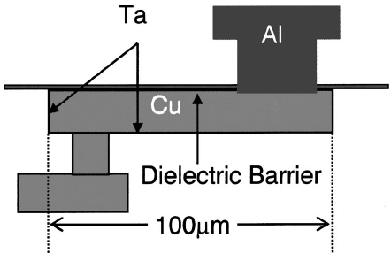
| Figure 2906a shows cross-sectional schematic illustration of Cu (copper) single damascene interconnects with Ta barrier and dielectric diffusion barrier SiCxNy.
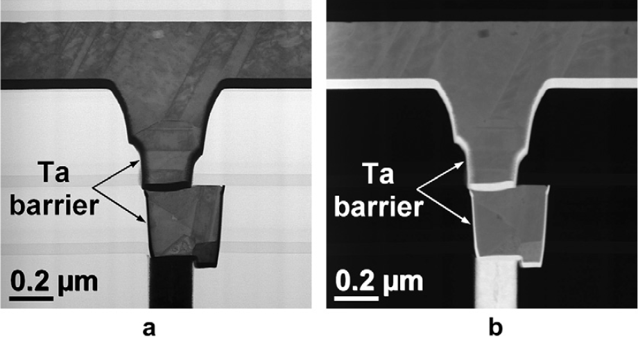
The Ta (tantalum) barrier shown in Figure 2906b plays a critical role in the copper dual inlaid process, which involves embedding copper lines and vias within a dielectric material. The Ta barrier is essential to prevent the diffusion of copper atoms into the surrounding dielectric or active areas of the device, which could degrade performance and reliability. The STEM (Scanning Transmission Electron Microscopy) images, particularly the HAADF-STEM image, clearly delineate the Ta barrier layer under the copper lines. This barrier layer ensures the integrity of the copper interconnects by providing a stable interface and blocking copper migration. The effectiveness of the Ta barrier in achieving uniform and thin layers is crucial for maintaining the overall electrical performance and preventing electromigration or other failures in the copper interconnects. Accurate measurement of the barrier thickness is important for process control, especially as device features continue to scale down. The HAADF-STEM imaging method allows for high-contrast imaging of heavy elements like Ta, making it an ideal tool for evaluating the barrier layer’s uniformity and thickness, ensuring it meets the stringent requirements of advanced semiconductor devices.
[1] T. Usui, H. Nasu, T. Watanabe, H. Shibata, T. Oki, and M. Hatano, Electromigration diffusion mechanism of electroplated copper and cold/hot two-step sputter-deposited aluminum-0.5-wt% copper damascene interconnects, Journal of Applied Physics 98, 063509 (2005).
|