Chapter/Index: Introduction | A | B | C | D | E | F | G | H | I | J | K | L | M | N | O | P | Q | R | S | T | U | V | W | X | Y | Z | Appendix
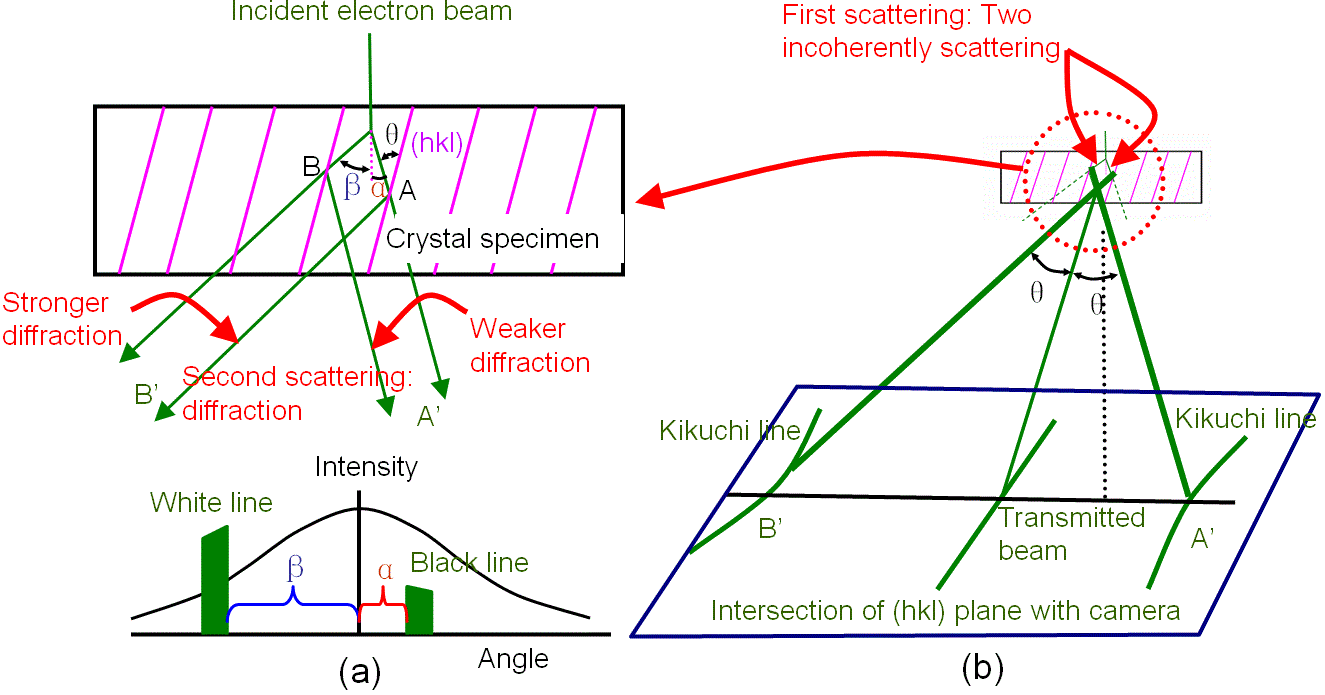
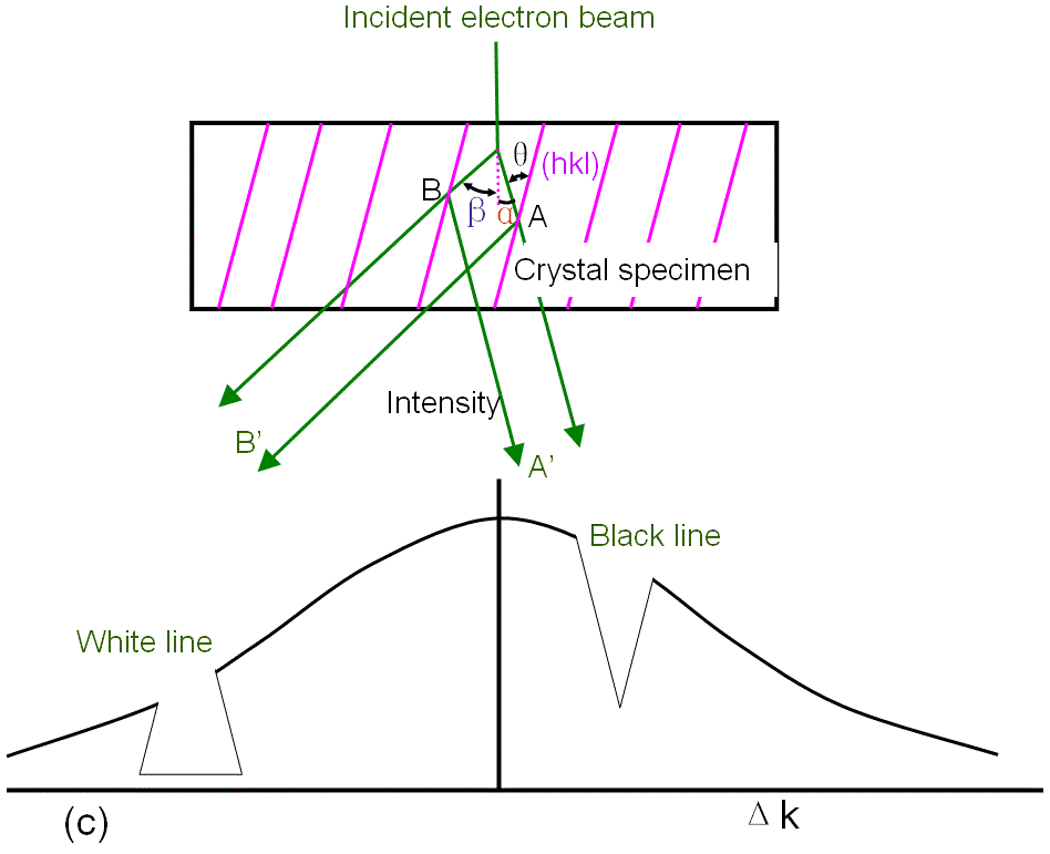
| When an X-ray beam irradiates a perfect crystal the absorption of the characteristic diffraction spectra from the crystal produces deficiency lines on the scattering pattern, known as Kossel lines. The same phenomenon occurring in electron diffraction is called Kikuchi lines. Kikuchi patterns appear in both SEM and TEM. Kikuchi lines in TEM normally give more accurate orientation determination than electron diffraction patterns. These Kikuchi lines may be either bright or dark, but they are straight and regularly arranged. Kikuchi lines originate with two electron scatterings: the first scattering is incoherent (sometimes inelastic), and then it is followed by a coherent (elastic) Bragg diffraction. TEM: For TEM, Kikuchi lines are paired black-white lines and are formed in addition to, or instead of, diffraction spots when a thick TEM specimen is used. Each of the Kikuchi lines corresponds to the diffraction spot, and thus can be indexed. The mid-line of a Kikuchi pair for (hkl) planes in Figure 4130a (b) corresponds to the intersection of the extension of the (hkl) plane with the camera or recording film. Figure 4130a is a simplified illustration; however, in reality, the intensities of Kikuchi lines are more complicated since the primary incoherent scattering may have multiple sources, and thus dynamical diffraction theory with absorption is needed for the intensity explanation.
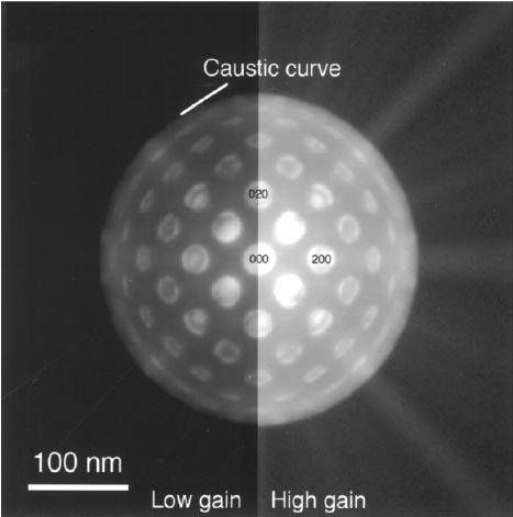
Kikuchi lines are more pronounced in CBED patterns than in SAD patterns because: i) CBED patterns arise from a smaller, and thus more uniform region than SAD patterns; and ii) The enhancement of coherent and elastic scattering in CBED. Figure 4130b shows an underfocus TEM image of a (001) SrTiO3 crystal with an incident probe focused on the specimen. The caustic curve is also indicated in the figure. High-angle thermal diffuse scattering is observed as Kikuchi bands, yielding background and a caustic curve.
Although Figure 4130b appears to be convergent-beam electron diffraction patterns, it is TEM images at a magnification of 1E5 with a defocus of about +5 µm. SEM: In SEM, the method of electron backscatter diffraction (EBSD) has been developed [1 - 5], while in TEM, the method of convergent beam electron diffraction (CBED) has been established. The intensity variation in a Kikuchi band in both CBED and EBSD patterns partially reflects the connection between the position of the localized scattering event within the crystal unit cell and the observed wave vector direction. Because the Kikuchi patterns in both cases are tied to the local crystallographic structure in the probing area, the patterns can provide important crystallographic and phase information down to the nanoscale in materials science. More accurately speaking, these patterns exist as a network of lines and bands. The information of Kikuchi bands is in principle provided by the combination of low angle elastic scattering with inelastic scattering. The lines appear straight rather than as curved lines due to the shorter wavelength of the electron beam. The kikuchi lines may be either bright or dark, but are extremely straight and regularly arranged.
[1] Schwarzer, R.A. (1997) Automated crystal lattice orientation mapping
using a computer-controlled SEM. Micron 28, 249–265.
|