Chapter/Index: Introduction | A | B | C | D | E | F | G | H | I | J | K | L | M | N | O | P | Q | R | S | T | U | V | W | X | Y | Z | Appendix
| Linewidth Roughness (LWR) and Line Edge Roughness (LER) are both important parameters in semiconductor manufacturing, particularly in MOS transistors, where precise control of feature dimensions is essential for performance and reliability. LER specifically refers to the variation in the position of a single edge of a feature, rather than the overall width. It represents how much a single edge of a line or gate meanders or fluctuates from its intended straight path. Like LWR, LER is caused by imperfections during lithography and etching. These variations are more noticeable in smaller nodes and can affect the consistency of electrical properties across a chip. LER impacts the precision of the gate’s shape and ultimately its performance, especially in terms of variability in switching speeds, leakage, and overall transistor performance. A rough edge can introduce unwanted variability in the device’s operation. LWR refers to the variation in the width of a patterned feature, like a transistor gate, along its length. In other words, if we measure the width of a line at different points along its length, we may find that it is not perfectly uniform—it fluctuates. This fluctuation is known as linewidth roughness. LWR arises due to imperfections in the lithography and etching processes used to define features on the chip. These processes may leave unintended variations in the critical dimensions (CD) of the gate or other features, affecting the performance of the device. As the size of transistor gates shrinks in advanced process nodes, even small variations in the width can have a significant impact on electrical characteristics such as leakage current and threshold voltage. This makes LWR a crucial factor to control in high-performance IC manufacturing. Roughness at wavelengths (or frequencies) large compared to diffusion lengths affects the shape of the doped volume, while shorter wavelength roughness affects the dopant concentration gradient. Here, the wavelength of roughness refers to the distance over which these fluctuations in the edge or width of a feature repeat. It represents the scale of the roughness, which can be either large (long wavelength) or small (short wavelength). Long wavelength roughness versus short wavelength roughness [1]:
If the edges of a line are uncorrelated, meaning the variations in one edge do not directly influence the variations in the other, the relationship between LER and LWR is given by the following equation:
Equation 9a (as shown in Figure 9a) implies that the roughness in the position of one edge (LER) is less than the roughness in the line’s overall width (LWR) because LWR takes into account both edges of the line. The factor of √2 comes from the assumption that the edges are uncorrelated, leading to a reduction in the measured roughness when focusing on just one edge.
Figure 9a. Relationship between LER and LWR. In practice, the roughness is to be measured over a range of wavelengths, starting from a minimum spatial wavelength defined by . [1] The residual, , which represents how much each measured point deviates from the ideal line (best-fit line), can be given by,
where,
The residual, wi, which represents how much each measured point deviates from the ideal width, can be given by,
where,
The residuals are used to compute the roughness metrics, which quantify how much the edge or width fluctuates along the length of the line. Figure 9b shows an example of residual xi at different edge position i along the line. The best-fit line typically represents a constant value along the length of the feature, particularly for uniform structures like edges or widths of lines.
Note that, there are non-typical cases where the best-fit line might not be constant, such as tapered features, systematic edge shift, non-uniform structures, process-induced nonlinearities, defect-induced deformation, and purposefully variable structures. While major CD-SEM suppliers now provide a range of LER measurement solutions, there is still no standardization in definitions and sampling capabilities. The commonly available measurement metrics include combinations of LWR, single-edge LER, total LER (calculated by summing the two edges in quadrature), and range roughness. Several critical metrics can be used to quantify line edge roughness (LER) and line width roughness (LWR). The Range measures the difference between the maximum and minimum deviations of the edge or width for a given segment. Average roughness calculates the arithmetic mean of these deviations from the best-fit line, providing a simple measure of roughness. Mean square roughness further refines this by calculating the quadratic deviations, offering a standard deviation-based understanding of roughness. Another key measurement is the Amplitude Density Function (ADF), which describes the probability distribution of the roughness, allowing for a more detailed statistical analysis. The Power Spectral Density (PSD) is also crucial, as it breaks down how roughness is distributed across different spatial frequencies, helping to understand how variations occur over different wavelengths. Lastly, the Autocorrelation function and correlation length provide insights into the spatial relationships between edge deviations, identifying characteristic distances over which roughness remains correlated. The average roughness (Ra) can be calculated by,
where,
For the data presented in Figure 9b, the average roughness (Ra) is 0.40 nm. The ADF can be plotted using the histogram of the residuals, which represents the probability distribution obtained by binning the residuals (xi) given by,
where,
For instance, Figure 9c shows the ADF obtained from the residual xi at different edge position i along the line.
In LER or LWR analysis, the PSD provides important information about how much roughness is present at various wavelengths along a line or feature. The PSD is derived from the Fourier transform of the measured edge positions (or widths). The Fourier transform breaks down the roughness into different frequency components, and the PSD shows the power (or amplitude squared) associated with each frequency component. PSD helps quantify how different spatial frequencies contribute to the overall roughness. By examining the PSD, one can determine whether the roughness is dominated by long-wavelength or short-wavelength features. This is useful for understanding the impact of roughness on semiconductor devices, as different frequency components of roughness can have different effects on device performance (e.g., long-wavelength roughness might affect doping, while short-wavelength roughness might influence the concentration gradient of dopants). For a series of measured residuals wi, the PSD can be computed using the coefficients of the discrete Fourier transform, [2]
The PSD for each frequency component is then,
where,
The area under the PSD curve is related to the root mean square (RMS) roughness, and specific ranges of spatial frequencies can be analyzed to understand the contribution of different frequencies to the total roughness. Figure 9c shows the power spectral density of residuals presented in Figure 9b.
As mentioned above, spatial Frequency refers to how often a particular feature (or variation in the roughness) repeats over a given length. It is measured in cycles per unit length (e.g., cycles per nanometer):
Random errors (noise) in the image can affect the accuracy of roughness measurements. Specifically, these errors impact the determination of edge positions or linewidths when using an edge assignment algorithm. The measured roughness is the sum of squares of the measured widths (which include both the true widths and the noise), which is represented mathematically by,
where,
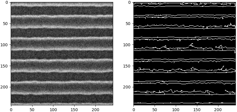
The effect of noise is that it increases the measured roughness by an amount proportional to σϵ2, which is the variance of the noise. Figure 9d shows a CD-SEM image with the measured edges. The computed LWR from the original image is 74.82 nm, and the LER is 58.66 nm.
[1] Determination of Optimal Parameters for CD-SEM Measurement of Line Edge Roughness, Proceedings of SPIE - The International Society for Optical Engineering, DOI: 10.1117/12.535926, 2004.
|


 --------------------------------------------------------------------- [9d]
  --------------------------------------------------------------------- [9e]
 --------------------------------------------------------------------- [9f]
  --------------------------------------------------------------------- [9i]