Chapter/Index: Introduction | A |
B |
C |
D |
E |
F |
G |
H |
I |
J |
K |
L |
M |
N |
O |
P |
Q |
R |
S |
T |
U |
V |
W |
X |
Y |
Z |
Appendix
Electron Diffraction of Erbium Silicides
| Table 977. Electron diffraction of erbium silicides.
| Erbium silicides |
Electron diffraction |
| ErSi2-x |
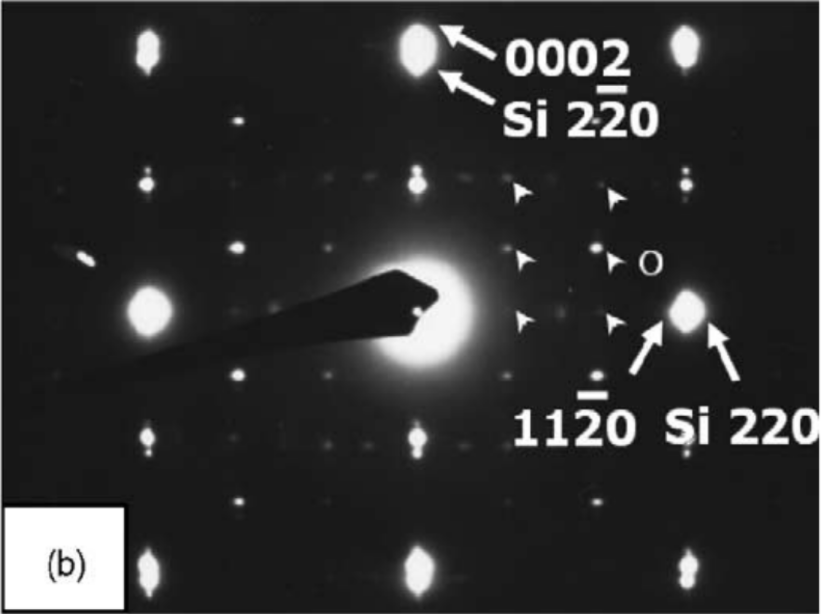
Diffraction pattern of a planview TEM sample of ErSi2-x on Si(001) annealed at 700 °C. The extra spots are due to ordered vacancy structure are marked by "O". [1] |
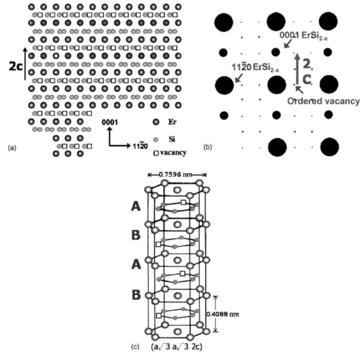
Schematic plots showing: (a) the ordered vacancy structure, (b) a simulated electron diffraction pattern viewed along the [1-100] silicide direction and (c) three-dimensional vacancy ordering structure. The vacancy positions are indicated as empty squares. [1] |
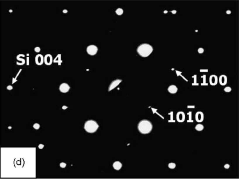
Diffraction pattern of a cross-sectional TEM sample of ErSi2-x on Si(001) annealed at 700 °C. [1] |
[1] W.C. Tsai, H.C. Hsu, H.F. Hsu, L.J. Chen, vacancy ordering in self-assembled erbium silicide nanowires on atomically clean Si(001), Applied Surface Science 244 (2005) 115–119.
|
