Chapter/Index: Introduction | A |
B |
C |
D |
E |
F |
G |
H |
I |
J |
K |
L |
M |
N |
O |
P |
Q |
R |
S |
T |
U |
V |
W |
X |
Y |
Z |
Appendix
TEM Imaging of Gadolinium Silicides
| Table 981. TEM imaging of gadolinium silicides.
| Gadolinium Silicides |
TEM images |
| GdSix |
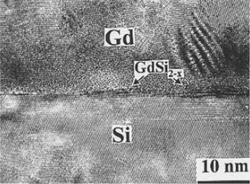
Gd thin film deposited on (111)Si annealed at 150 °C. There is an amorphous interlayer (a-interlayer) and nucleation of the crystalline silicide. [1] |
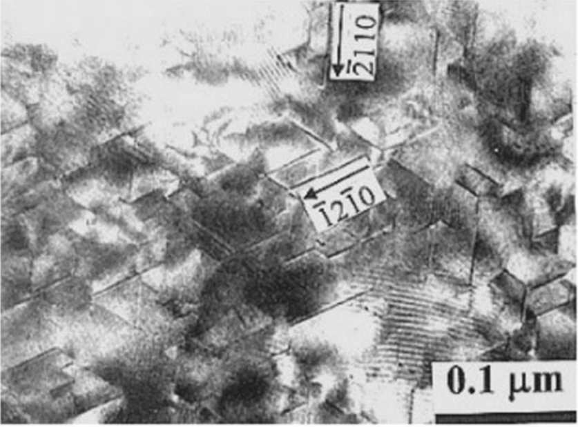
| GdSi2-x |
Gd/Si(111) samples annealed at 600 °C for 1 min. [1] |
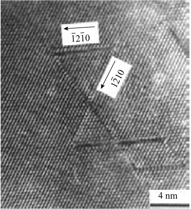
Planar stacking faults, on {10-10} planes, along three <-12-10> and <0001> directions in epitaxial GdSi2-x thin films viewed along the [0001] direction. [2] |
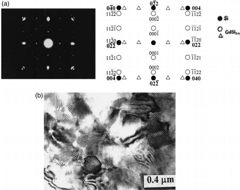
Coexistence of epitaxial H(hexagonal)-GdSi2-x and polycrystalline O(orthorhombic)-GdSi2 in a Gd/(001)Si sample annealed at 600 °C: (a) polycrystalline O-GdSi2 rings and two sets of epitaxial H-GdSi2-x (see page2036_f), with orientation relationships between H-GdSi2-x and (001)Si, which are (A) (1-100)GdSi2-x/(001)Si with [0001]GdSi2-x/[2-20]Si and (B) (1-100)GdSi2-x/(001)Si with [11-20]-GdSi2-x/[2-20]Si. The two sets of GdSi2-x are crystallographically equivalent with one rotating 90° relative to the other around the common [1-100]GdSi2-x axis. Two perpendicular
orientations with the same Moire fringe spacings, indicating that the epitaxial films tend to orient with two different azimuthal orientations rotated by 90° with each other. [1] |
[1] J.C. Chen, G.H. Shen, L.J. Chen, Interfacial reactions of Gd thin films on (111) and (001) Si, Applied Surface Science 142 (1999) 291–294.
[2] Lih J. Chen, Silicide Technology for Integrated Circuits, 2004.
|
