Chapter/Index: Introduction | A |
B |
C |
D |
E |
F |
G |
H |
I |
J |
K |
L |
M |
N |
O |
P |
Q |
R |
S |
T |
U |
V |
W |
X |
Y |
Z |
Appendix
Electron Diffraction of Nickel Silicides
| Table 986. Electron diffraction of nickel silicides.
| Nickel silicides |
Electron diffraction patterns |
| NiSi2 |
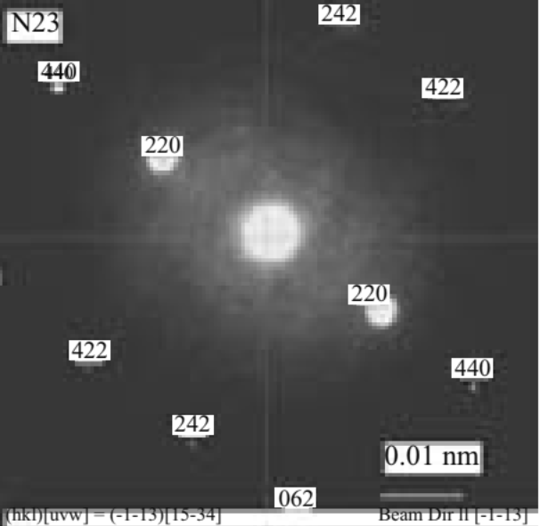
Micro-diffraction of NiSi2 [1] |
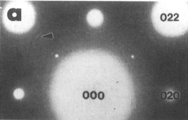
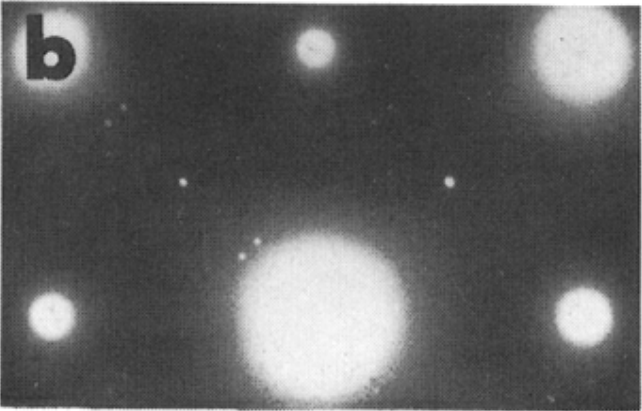
Complicated reconstruction at NiSi2/Si(100) interface: (022) spots from both Si
and NiSi2; (020) from
NiSi2alone; (0, 1/2, 1/2) from superstructure(s) at the NiSi2/Si interface; diffuse spots or streaks for thick NiSi2 in Figure (a) are related to both (0, 1/2, 1/2) and (0, 1/2, -1/2), originating from domains related by a 90° rotation (a higher temperature and/or a longer time anneal leads to the appearance of discrete spots slightly displaced from the (0, 1/2, 1/2) and (0, 1/2, -1/2) positions). Arrows
point to positions equivalent to (0, 1/2, 1/2). [2]
|
[1] Lih J. Chen, Silicide Technology for Integrated Circuits, 2004.
[2] R. T. Tung, Epitaxial CoSi2 and NiSi2 thin films, Materials Chemistry and Physics, 32 (1992) 107-133.
|