Chapter/Index: Introduction | A |
B |
C |
D |
E |
F |
G |
H |
I |
J |
K |
L |
M |
N |
O |
P |
Q |
R |
S |
T |
U |
V |
W |
X |
Y |
Z |
Appendix
XRD of Nickel Silicides
| Table 987. XRD of nickel silicides.
| Nickel silicides |
XRD profiles |
| NixSiy |
From [1] |
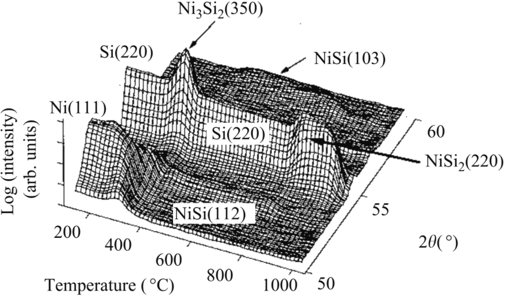
Three-dimensional (3-D) rendering of the in situ X-ray diffraction
measurements during annealing of a 15 nm Ni film deposited on p-doped
poly-Si (3 °C/s). [2] |
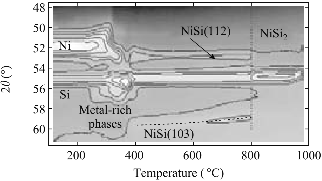
In situ X-ray diffraction
measurements during annealing of a 15 nm Ni film deposited on p-doped
poly-Si (3 °C/s). [2] |
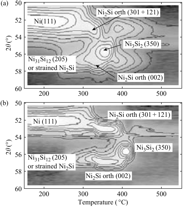
In situ XRD measurement during annealing of a 15 nm Ni film
deposited on (a) p-doped and (b) n-doped SOI substrate. [2] |
| NiSi |
Coefficient of thermal expansion (CTE) (orthorhombic structure) [3]:
a = 0.5187 − 1.807 × 10⁻⁵T + 6.026 × 10⁻⁸T2 − 2.709 × 10⁻¹¹T3 (nm)
b = 0.3286 + 2.977 × 10⁻⁵T − 6.557 × 10⁻⁸T2 + 2.915 × 10⁻¹¹T3 (nm)
c = 0.5626 − 1.779 × 10⁻⁵T + 5.727 × 10⁻⁸T2 − 2.546 × 10⁻¹¹T3 (nm) |
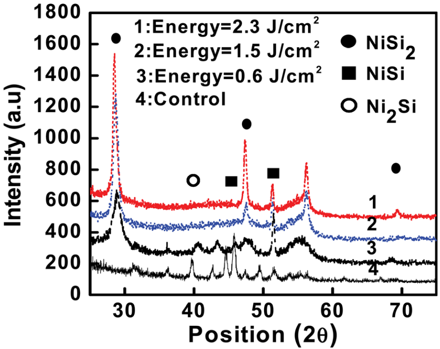
[1] Hou-Yu Chen, Chia-Yi Lin, Min-Cheng Chen, Chien-Chao Huang, and Chao-Hsin Chien, Nickel Silicide Formation using Pulsed Laser Annealing for nMOSFET Performance Improvement, Journal of The Electrochemical Society, 158 (8) H840-H845 (2011).
[2] Lih J. Chen, Silicide Technology for Integrated Circuits, 2004.
[3] D. F. Wilson, O. B. Cavin [Scripta Metall. Mater. (Netherlands), 26,
p.85, (1992).
|
